This is a project to make something that can be used to work out calibration details for a clock/calendar chip and measure frequencies with a reference having 5-10ppb frequency stability. This isn’t to break any new ground. Frequency counters have been around forever and RTC clock calibration is well understood. I’m doing this as an exercise to get more experience as well as making some tools for long term use.
Here are my goals:
- Making a tool chain to quickly and easily calibrate and arrange runtime temperature compensation for a few clock chips:
- ST M41T62
- DS 3207
- DS 3231/34
- Designing the logic for a non-trivial, bus-oriented microcontroller driven peripheral
- Getting more experience with high speed circuits
- Getting started with Kicad (the free version of Eagle isn’t going to cut it for this system)
- Getting to the point where the Dangerous Prototypes “Logic Sniffer” logic analyzer is a tool about as familiar as a screw driver
And stretch goals:
- One or more class libraries for calibration that are general and portable enough to be interesting to others
- Fix some of the problems with the logic sniffer client code, starting with the stability issues causing transient “device not found” errors
Caveat
This document is being added to at the bottom with little or no effort to go back and adjust the earlier bits to make them consistent as I change my mind about 700 times about details. (e.g. as I was typing this I peaked ahead a few paragraphs and I’m a bit shocked by how much things have changed!). Apologies in advance for the poor “flow”. Also, this was started in 2014 and parked from early 2015 for a year. It’s resuming in March, 2016. I’ve got a rubidium standard, HP5335A counter, nice mixed signal oscilloscope, but I still haven’t dived into Kicad.
But I did double back to add this caveat and a list of “nearly finished” circuits:
So now, pretend it’s the summer of 2014…
Design
The hardware described below and a handful of gpio ports on a microcontroller (or maybe a Raspberry Pi) are aimed at two functions:
- Counting the ticks of an arbitrary digital signal source for precisely measured lengths of time. Initially the signal source will go through a 74HC125 buffer and straight into a 32 bit counter that’s gated by an oven controlled crystal oscillator (A Raltron OX6580A-LZ-10-10.000-12) divided down by a chain of decade counters. Later some simple prescaling will be added to allow for counting faster than the 74HC chips can go without scaling.
- Counting ticks of the 10mhz OCXO while counting down ticks of an external clock source (e.g. an RTC clock’s “squarewave output”) with a divide by N counter. Prescaling of the external source will be added later. The basic idea, for example, is to count down N ticks from an RTC chip while counting up 10mhz ticks from the OCXO. For example, counting 16384 ticks from an RTC’s 32k squarewave output should involve 5 million ticks from the 10mhz clock. If instead there were 5000005 ticks the RTC would be one part per million slow, while if there were 4999995 ticks the RTC would be one part per million fast. Counting more RTC ticks will allow for more precision up to limit imposed by the OCXO performance. The 32 bit counter is good for about six minutes of timing, which is plenty.
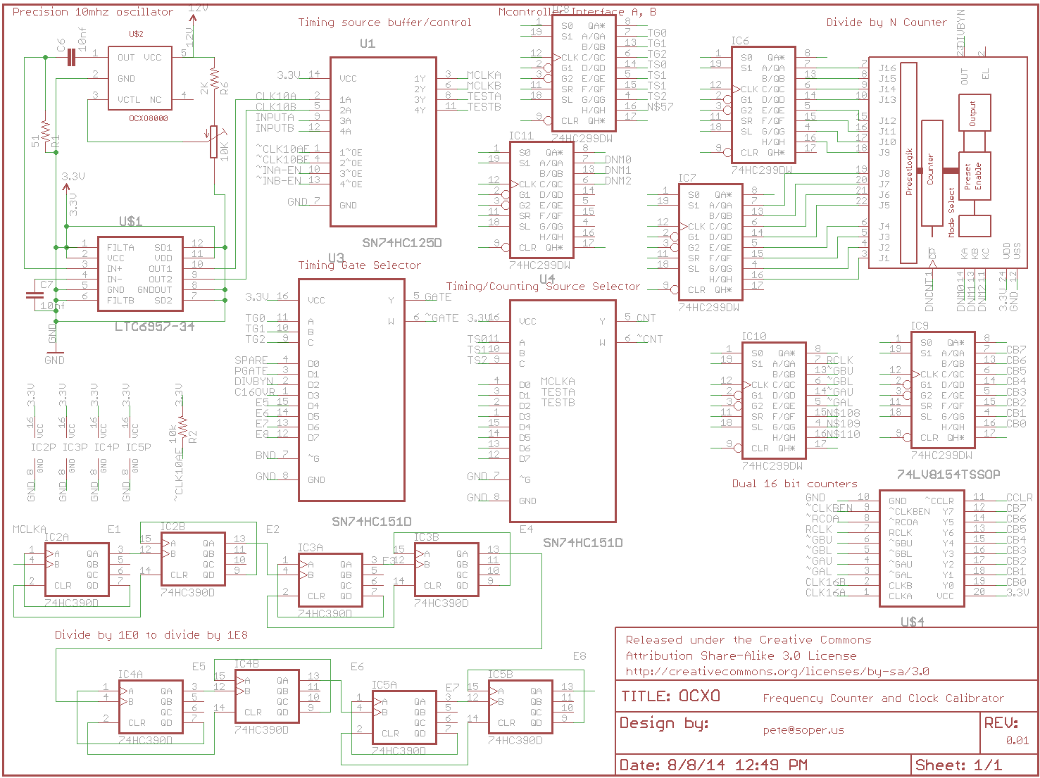
The hardware will be mostly 74HC CMOS running at 3.3v. The OCXO feeds a Linear Technology LTC6957-3 chip that converts the oscilator’s sine wave to CMOS-compatible square wave. A Schmidt converter cleans the square wave up and from there it goes through a 74HC125 buffer with active low enables. A set of four 7HC390 dual decade counters divide the 10mhz clock and provide time base signals out to one per 10 seconds. A 74LV8154 32 bit counter will accumulate 10mhz clock pulses and make the count available in four pieces on a bidirectional eight bit bus. The “jam count” for the divide by N counter (74HC4059) is loaded with a pair of 74HC299 shift registers. Other 74HC299 registers will drive control signals, such as sets of three bit codes into 74HC151 one of eight selectors to determine which decade counter output provides the time base for frequency counting, which signal source drives the timing gate, etc. Bus transceivers and latches and a small pile of synchronizers and combinatorial logic will fill the design out. About half the target hardware is on a large solderless protoboard at this point. The Eagle design with pending death sentence and missing gobs of bypass caps, pullups, signal names, etc, for lack of room looks like this:
Rev 0.01
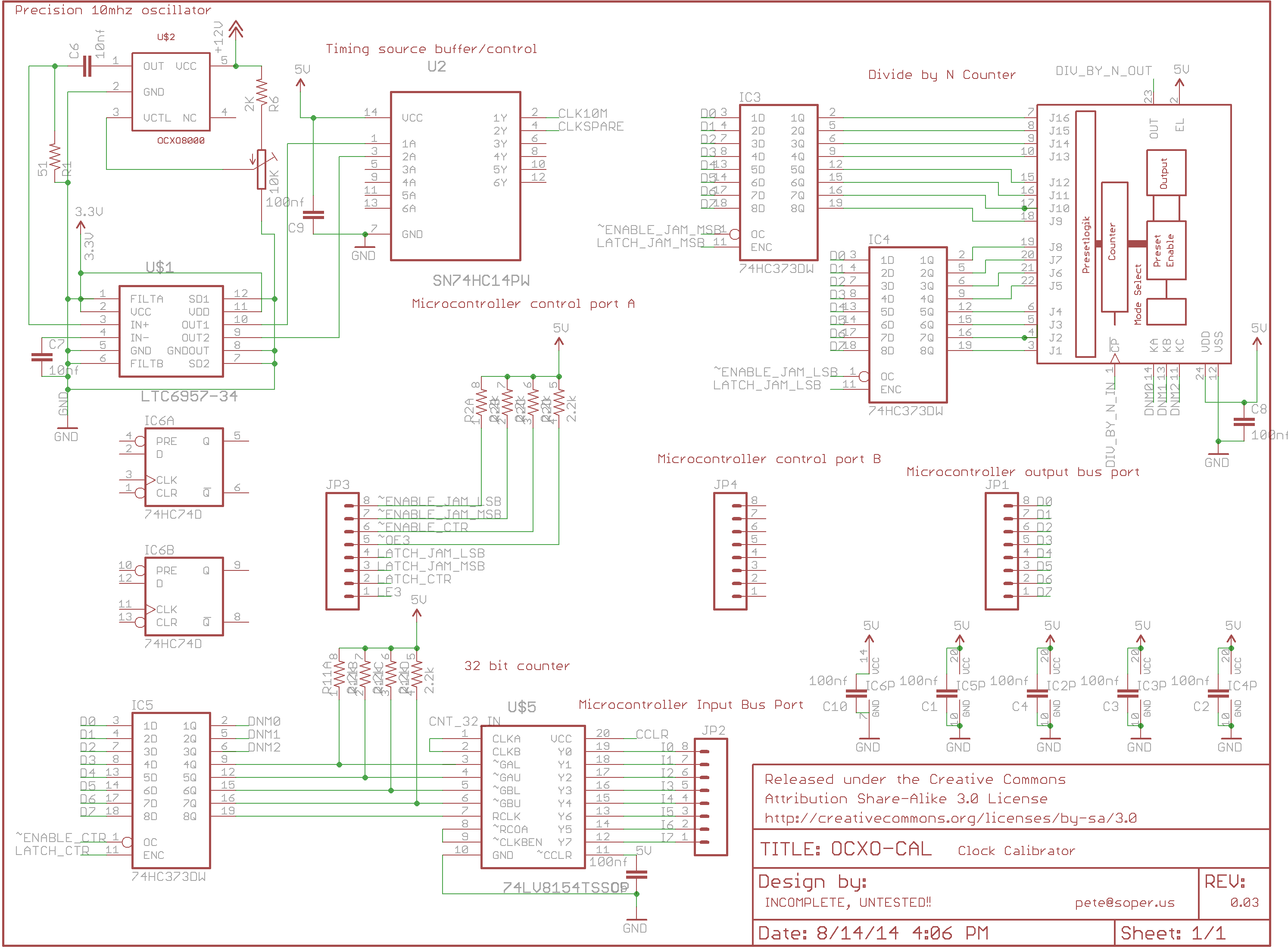
I’ve set the frequency counter aside for the being (after realizing “Duh: ripple counters won’t do the job!” and to try to fit the calibrator into one page. Here’s the latest (but still incomplete and untested).
Rev 0.03
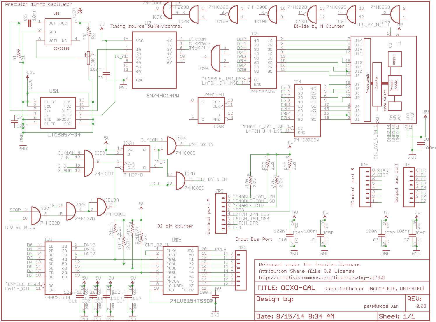
Next I turned attention to how to gate the OCXO clock into the 32 bit counter and the test clock (e.g. a 32khz square wave from an RTC chip) into the divide by N. The gate needs to turn the clock sources on the point where both are providing a leading edge to trigger the 74hc74 D flip flop. Since the OCXO clock is running about 300 times faster than the highest RTC square wave rate I expect to encounter, I figure the leading edges may coincide regularly. This may be completely wrong: I just don’t know. I might wait seconds, minutes, fortnights for a coincident leading edge, but I’m willing to go ahead and try this instead of digging through reference material or asking questions to find out the answer (there are folks who no doubt know very well how likely these clocks are to get synchronized for a single cycle start. Another issue that’s itching my brain is the propagation delay through the divide by N counter and the “slop” in its delivery of the completion pulse when (for example) the 32768th test clock pulse has completed. Actually, I think I’m looking for the leading edge of the 2769th cycle, if I’ve properly thought this through. But for the sake of cramming the prototype onto one large protoboard I’m going to stick with the divide by N for now. So here’s what it looks like at the moment. The row of backwards-facing gates are ones that are currently unassigned. I’ll come up with a verbal description of what I’m expecting to happen with this logic with the next rev.
Rev 0.05
After a little thought it seemed clear that the actual coincidence of the two clock rising edges could be a very rare event. On the other hand, it was the AND gate taking the two clock signals in, and perhaps the overlap would generate a rising edge to feed the flip flop readily. But then I did a little arithmetic and realized that the maximum error that I was trying to avoid was a shade under 100ns. Figuring the delay through the “stop” logic and the divide by N counter could add another 100ns and potentially cause an extra cycle into the 32 bit counter, that’s 200ns error. In one second of measurements that’s .2ppm!! This is a tiny fraction of the error in the OCXO itself. Hooookay, maybe synchronizing with both clocks is silly. By just starting the counters on the leading edge of the test clock everything gets simpler:
Rev 0.06
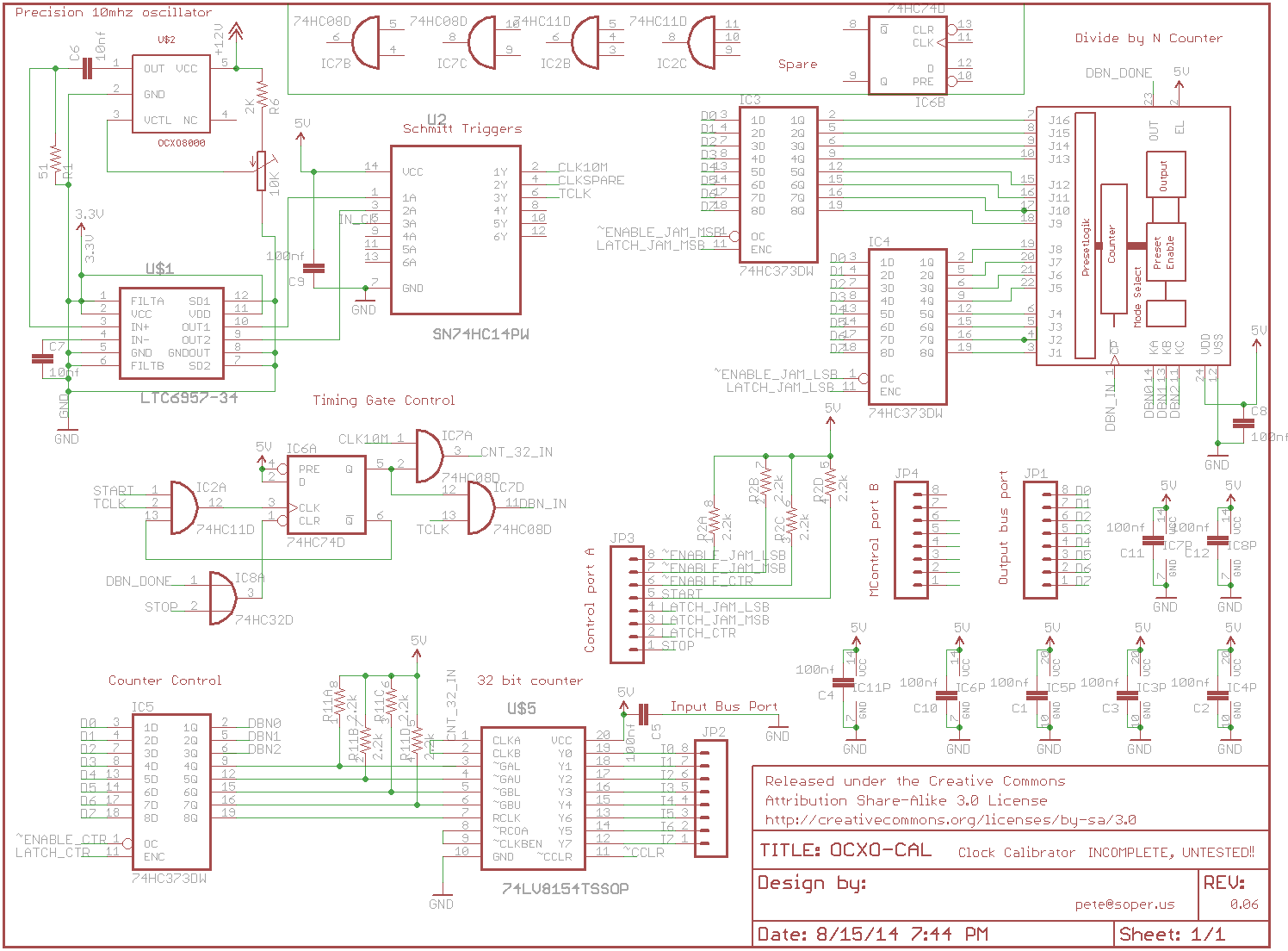
It occurred to me that there are schmitt trigger logic gates so I could switch to schmitt NOR gates and eliminate the 74HC14. (Note that the schematic symbols for these 747002 gates stink, but I can be bothered to fix that and other sins, such as the 74HC74 clear being marked CLR instead of ~CLR.) I also realized that a single triple-input AND package would get the job done. I also realized the latches controlling command and preset signals to the counters could be permanently enabled and I simplified the intended microcontroller interfaces and added a level (i.e. vs edge triggered) interrupt to wake up a micro when the divide by N counter completes. Meanwhile, as I glance at the board side of the CAD program it occurs to me that this could be an expensive board. On the heels of that is the notion that creating multiple versions of the board for the sake of the OCXO and it’s signal conditioning and trim circuitry would be stupid because I only have one of those and don’t intend to solder and resolder that hardware. I’m going to put that into a separate little box with a screwdriver port for the trim pot, 12v supply jack and BNC jack for the 10mhz clock signal. (FINALLY going to use one of the dozens of BNC connectors I accumulated during my radio contesting years!) The other cost control strategy would be to switch from the easy to hand solder SOIC and TSSOP packages to denser packages where they’re available. That would save cost both by virtue of the smaller packages tending to be cheaper and reducing the fractional acres of PCB area. On the other hand, bugs are much harder to fix in this case because there is often no exposed pad of any kind on the board for a given circuit connection. So going with small packages would be a disaster if I needed very many wires to fix mistakes. I guess in theory the solder mask could be scraped off a trace and a wire could be soldered to it, but. my “ECO wire” (30 gauge kynar kept from the days of wire wrapping) is 10 mils in diameter: almost double the width of the smallest traces I’ll be using. To say this would be premature optimization would be an understatement. A few other details.
- Powering most or everything but the oven with 3.3 volts was looking marginal at every turn. It might still work, but life is short and has more noise margin at 5v.
- After a lot more searching it appears the 74LV8154 is it as far as interesting counters go. The ancient 4000 CMOS series has some counters, but they have drawbacks. Anybody else know of something like the 74LV8154 but with a freaking overflow out of the high order bits so a larger counter can be made? It annoys me to have to use the low order 16 bits of one of these to make a longer word length counter.
Here’s the circuit now. This is feeling pretty close to something I can finish putting together on a breadboard to try out.
Rev 0.07
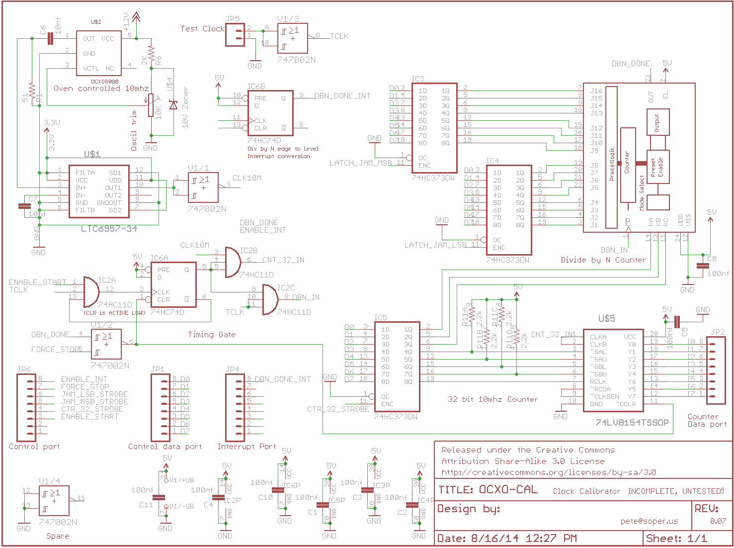 I realized I can get away with a single data bus because the latch controlling the commands to the 32 bit counter can be disabled with the latch output enable. So with care not to plug the wrong pattern of bits into the control/interrupt port from a microcontroller this circuit can alternately drive counter values onto or read commands/data off a single eight bit bus. If this works it will meet one of my major goals, which is to get experience with bus-oriented systems like this. So I only need 16 microcontroller pins:
- Seven for controlling the circuit
- One as an interrupt input for completion of the divide by N count
- Eight for I/O with the circuit
I’m wondering whether I should put some resistors in series with D0-D7 going to the microcontroller so that a case of “dueling outputs” doesn’t damage it. I guess some temporary logic making it impossible for any of the counter output enables to be low while any of the data bus lines are either high or low (i.e. not high-Z), but I’m not sure how to detect that. While meditating on this I’m finishing a Digikey order to get remaining parts to proceed with breadboarding. Here’s the latest.
Rev 0.08
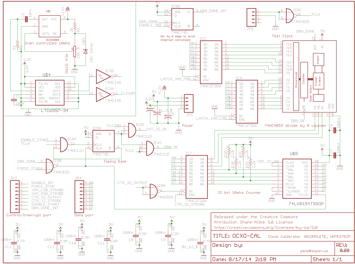
Oops. I thought I’d found a way to avoid a latch or clock or something with the 32 bit counter but the circuit above will drive the counter onto the bus at the same time the microcontroller is telling the counter which 8 bits to present to the bus. In addition, the ~CCLR line of the counter is going to be pulled low every time FORCE_STOP is asserted or the divide by N counter completes. Bzzzt, wrong. So I’ll decode the low order two divide by N counter control lines and when they’re both low to (pre)reset that counter the 32 bit counter will be cleared too. And one more latch will isolate the bus from the counter output. It’s output enable will just be the complement of the enable of the latch driving commands to the counter. I’m still concerned in case the microcontroller gets into a state where it drives a bad pattern of signals that cause multiple devices to be driving the bus at the same time. I think as long as I never, ever connect the circuit to some random microcontroller that has who-knows-what code running in it I’ll be OK. (Famous last words)
Hmm, speaking of, as I was preparing the next section I notice a potential problem. I had the 32 bit counter output latch enable wired so it would be low (driving the bus) when the control port is first initialized as an output. If this was done before this bit was driven high it would put both the microcontroller and and the latch as outputs driving. This would probably be harmless except then when trying to drive the enable high (to turn it off) it isn’t clear what would happen, as presumably the counter output latch would be holding the bus in a fixed state. So I reversed the sense and now when the counter command defaults to low (driving signals into the counter chip) the counter output latch is disabled and it’s output is in a high-Z state. So here’s another pass to fix the issues I just described.
Rev 0.10
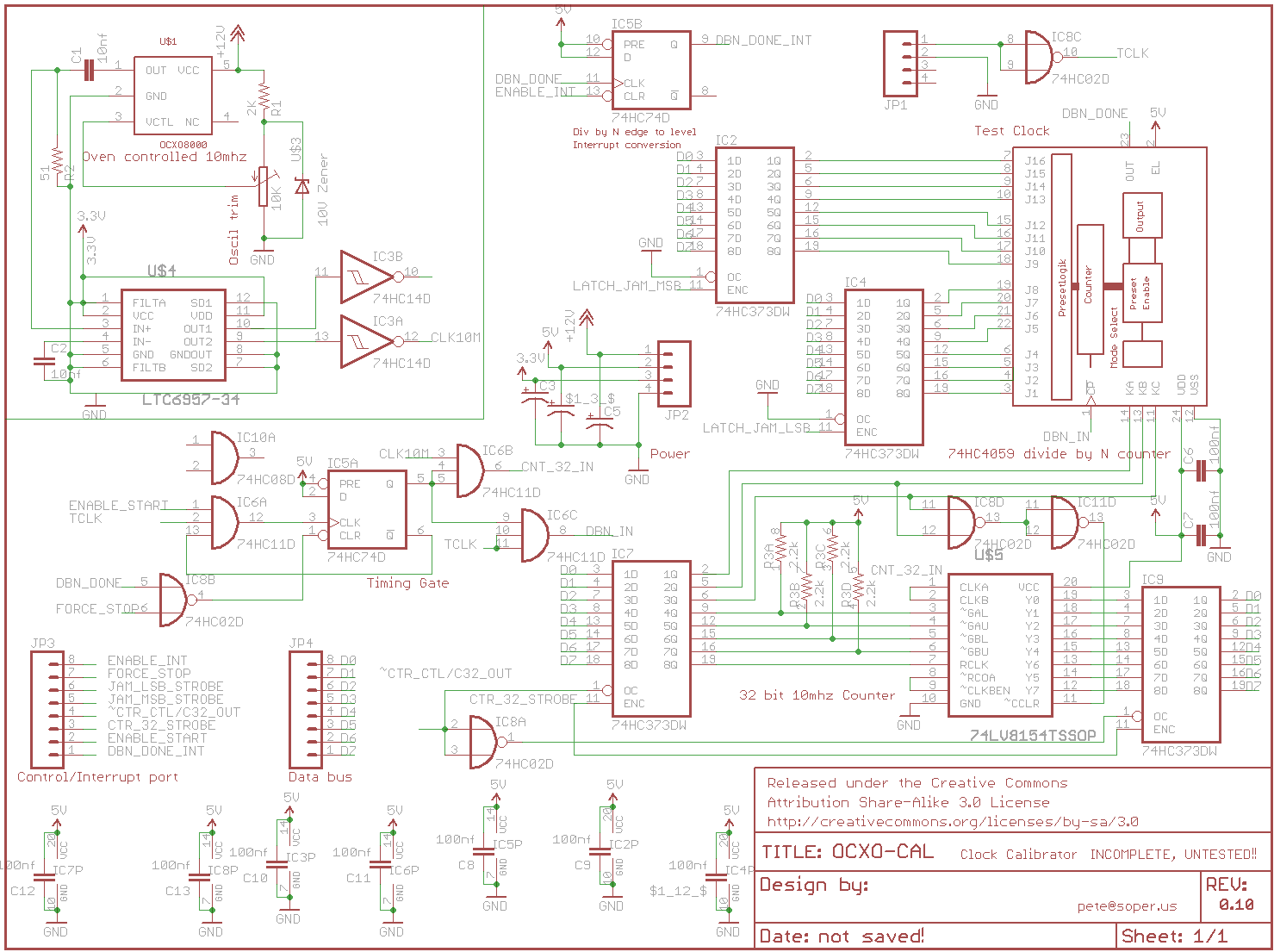
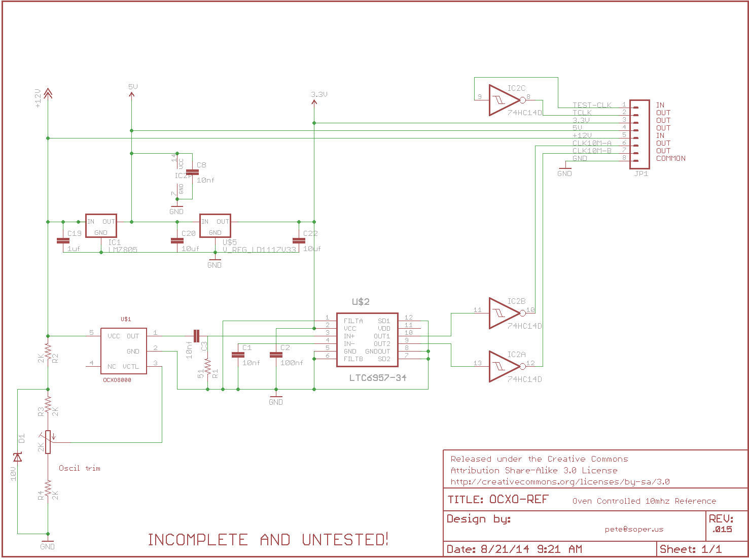
(Took a few days off to deal with other things) The schematic was getting too crowded, so I split off the OCXO 10mhz frequency source, power supply circuits, and a bit of signal conditioning for the “clock to be tested” into a separate schematic. This will get a few more details like proper connectors and live in a box as a stand alone device going forward.
Power/OCXO/Signal Conditioning Rev 0.15
So now the main piece of work is just the circuitry for measuring a test clock source using the precision source above.
OCXO-CAL 0.15
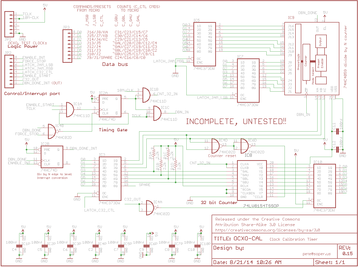
The “software interface” via two microcontroller ports is pretty well specified in the schematic above. The “control/interrupt” port will connect to seven output pins and one interrupt input pin of a micro while another eight lines will connect as the alternating outputs and inputs of a “data bus”. When some of the control port signals are driven the data bus lines are interpreted as preset values for the divide by N counter, reset and timing setup state etc. After a timing run other control line settings cause the circuit to drive different portions of the 32 bit counter value onto the data bus where it can be read.
The ticklish bit with this is avoiding scenarios where the circuit is commanded to drive some eight bit chunk of the counter value onto the bus while the microcontroller’s corresponding port is configured as an output. This would create a ‘dueling output gates’ situation where the right-most 74HC373 latch is trying to hold the bus lines in one set of eight states while the microcontroller is trying to hold them in a different state. My guess is that the latch chip will win the contest and the microcontroller gate transistors may lose their magic smoke. To make it less likely I won’t keep my mind right and accidentally arrange this kind of duel I’ve made all the control bits active high. I could have made them active low: the key thing is for them to all be consistent so a momentary lapse of concentration while writing or changing the software doesn’t tend to result in a duel.
Related to this issue is my flip-flopping over what supply levels I can use for the various circuits (except the LT6957 clock is strictly 3.3 volts only). And I’ve gone back to the MSP430 and would like nothing better than to run this circuit with one of those, but they are strictly 3.3 volt devices. So the next order of business is to determine if there might be logic level compatibility between an MSP430’s pins and all the various timing circuit devices, whether I want to try to run the circuit at 3.3v, or whether I want to break down and throw a level converter in between the two sets of eight circuit lines connecting to the microcontroller.
I know of a chip that seems to be the perfect level shifter, but it seems silly to use it if I don’t need it and can just be careful to avoid dueling output gates. It occurred to me that by guaranteeing only one of the ‘373 latches is active at a time (but this means “enabled” or “latched” depending on the chip) and that none are active when the corresponding micro control port is initialized I can probably minimize the hazard described above.
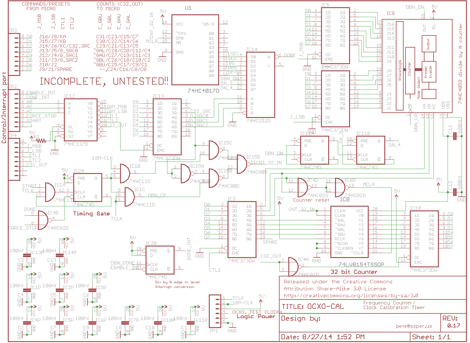
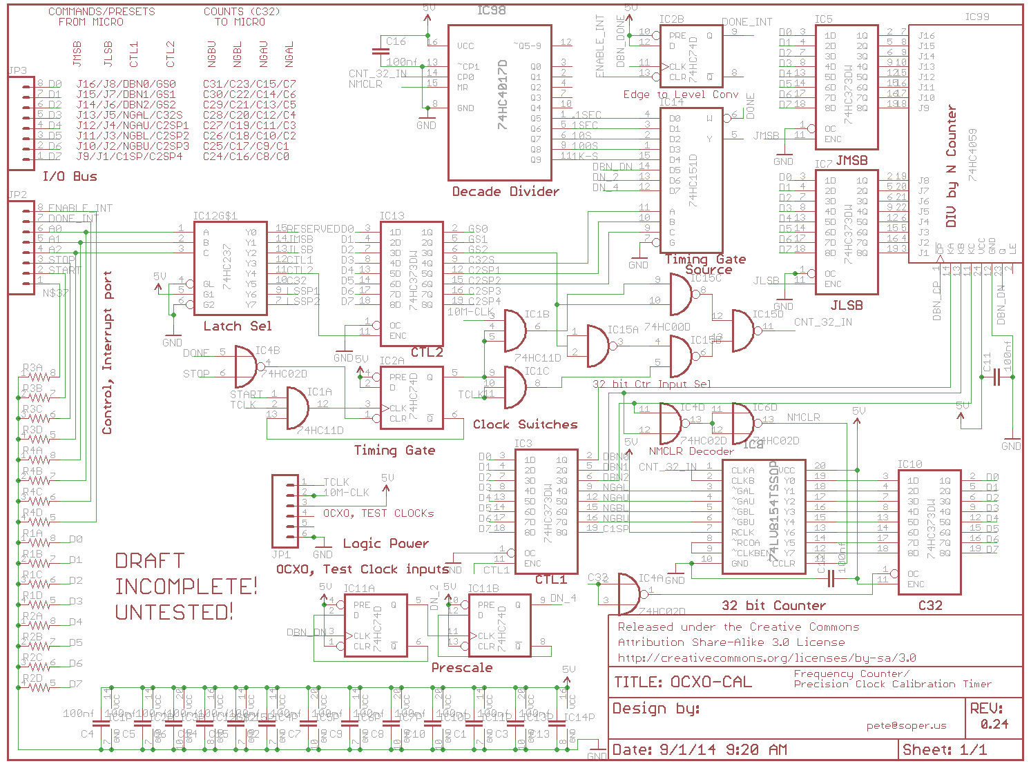
It also occurred to me that I really need a plain frequency counter and I almost convinced myself that this “divide by N” scheme for precisely measuring something like a second’s worth of test clock pulses was a waste. Then I realized it would take 1000 seconds of frequency counter measurement before I could measure a 32k square wave as accurately as one second’s measurement by just counting between a beginning and ending edge. I know that was confusing. The bottom line is that I may have crammed the frequency counter functionality back in, and I’ve for sure crammed a proper “command encoder” in to create the “only one latch at a time” behavior I want. Here’s the current version. There are for sure some typos/mistakes in this but I need to get it down before continuing.
OCXO-CAL 0.17
As I have many thoughts along the lines of “is it really going to be possible to wire this up and make it run on one breadboard?” I’m also thinking more about how a microcontroller will drive it and where to draw the line between smarts in the hardware vs the microcontroller software.
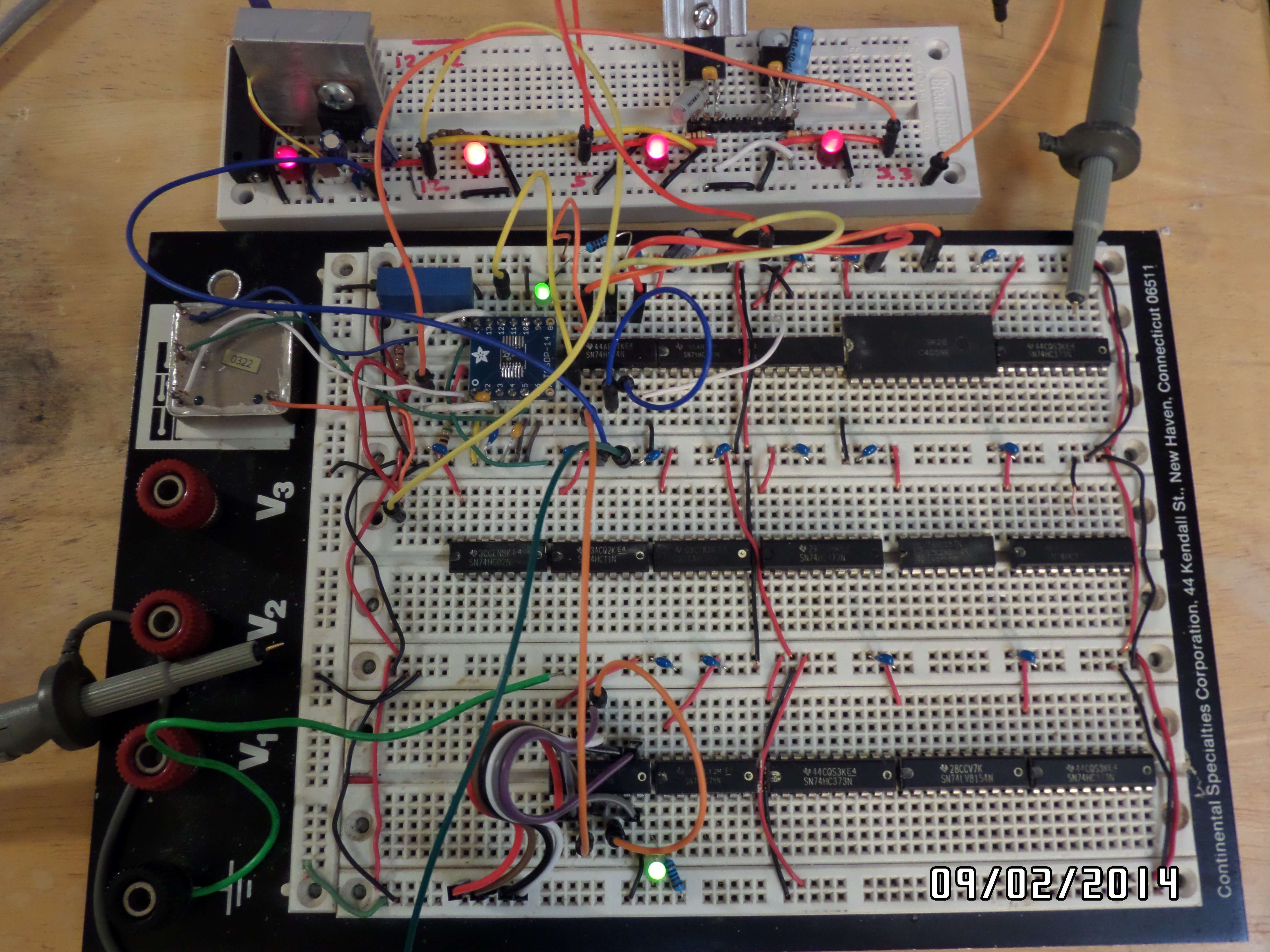
But that’s a pretty easy decision: no more hardware smarts will fit! In fact I’ve got a minor crisis in that it dawned on me that the eight bit I/O bus at a minimum, and for the care and well being of the chips on the board in general the seven control lines in addition will need pull-down resistors to avoid the terrible behavior of CMOS chips oscillating at very high frequencies. That is, these lines are at very high impedance and “floating” when the microcontroller is disconnected or not configured and also when the latch feeding the 74LV8154 counter output to the microcontroller bus is in a high-Z state and the microcontroller is configured to treat the I/O bus as eight input lines. According to a very nice TI design document I read recently it’s a fundamental no-no to allow inputs to float like this, as in the worst case a package with a lot of floating inputs can exceed it’s current draw (and thus thermal) limits in short order. (TLDR; note: page 9, “Pull up or pull down resistors” is the salient part of this document). So, that means 16 resistors tied to these lines to make sure they are connected to a power supply rail. Because it would be counter productive to have some of the lines default to “high” by design (e.g. it would direct the gate logic to both start and stop at the same time), the lines have to be tied through resistors to ground. For the I/O bus that would be a nice, neat operation if the 74hc373 was layed out “properly”: just stick a resistor SIP package in place with it’s eight resistors neatly connecting to the latches data lines and its ninth pin stuck into the latch’s ground connection. Except the original 74373 designers were cruel and thoughtless: the pins are not connected at all “correctly” for this convenience. In fact to my eye they are willy-nilly. (I’m joking. There was probably a lot of thought put into the pinout or else the designer’s hands were tied by manufacturing constraints or something at the time.) So I’m stuck with sticking resistors in breadboard pins and “jumpering” them into the appropriate parts of the breadboard and I’m concerned about the micro-acres of breadboard space that will involve. Here’s what the breadboard looks like. The PS regulation is “outboard” now, but not the OCXO and LTC6957-3, etc in the upper left corner. But when that’s moved out there will only be a few square inches of space recovered. I still need areas for logic analyzer and “little winking debug lights” or the like to be connected.
Breadboard snapshot
But back to the microcontroller interface. I went through the current design (below) and worked out the 37 steps required to run this circuit in “time between edge one and edge 32768 of a clock chip’s square wave” (that is, “divide by N”) mode. They look something like this sequence below.
- Set control bus lines to outputs, set up for interrupt line to be an active high, level sensitive interrupt
- Set I/O bus to outputs and put the most significant byte’s worth of bits on the bus for the divide by N counter’s “count jam” lines
- Strobe the control lines with A0-A2 to 0b001, that is a value of one (to pull the 74HC237’s Y1 output high). This one value will be called a “JMSB” command because it corresponds to the given 74hc237 line controlling one of the 74hc373 latches. A “strobe” just consists of setting the control line high values and then returning them to low immediately afterward. An 8mhz Atmega328 can do this in tens of microseconds: no worries about it being too fast for the 74HC-series logic chips! This command causes the 74hc373 latch feeding 74hc4059 lines “J9-J16” to latch its D0-D7 lines into a register (bunch of flip flops) to hold the outputs to the given values until further notice.
- (Same for JLSB)
- Set the I/O bus to 0b0001110 and strobe a “CTL1” command to force DBN0-2 low, which is seen by the 74hc4059 as a reset and decoded as a master clear (“MCLR”) by a 74hc02 to reset the 74hc4017 johnson counter and the 74lv8154 32 bit counter chip, while keeping that chip’s output enable lines off (NGAL, etc: active low enables).
- Set the I/O bus to 0b00101100 and use a “CTL2” command to:
- set C32_SRC high (forcing the selector made out of the 74hc00 nand gates to take clock pulses from the “10M-CLK” line fed by the (eventually) off-board OCXO system.
- Set the I/O bus to 0b11100000 and pulse a “CTL1 command”. This reflects the default “count down from 15999 to 17331” mode for the 74hc4059 divide by N chip and keeps the 74lv8154 chip’s counter output lines in a high impedance state.
- Etc.
In words, the other steps set up the next rising edge of the test clock to trigger the counting and then the 10mhz clock accumulates in the 32 bit counter (74hc8154) while the test clock counts the 74hc4059 down. When that counter finishes counting the 10mhz clock is cut off from the 32 bit counter and that counter’s contents can then be read out eight bits at a time.
In the “other mode” one of the Johnson counter outputs is used to time accumulation of test clock edges for a fixed length of time that’s as accurate as the 10mhz clock +/- propagation delays and the microcontroller will scale and present frequency measurements like common equipment provides.
And here’s the current schematic. Getting just a bit crowded now.
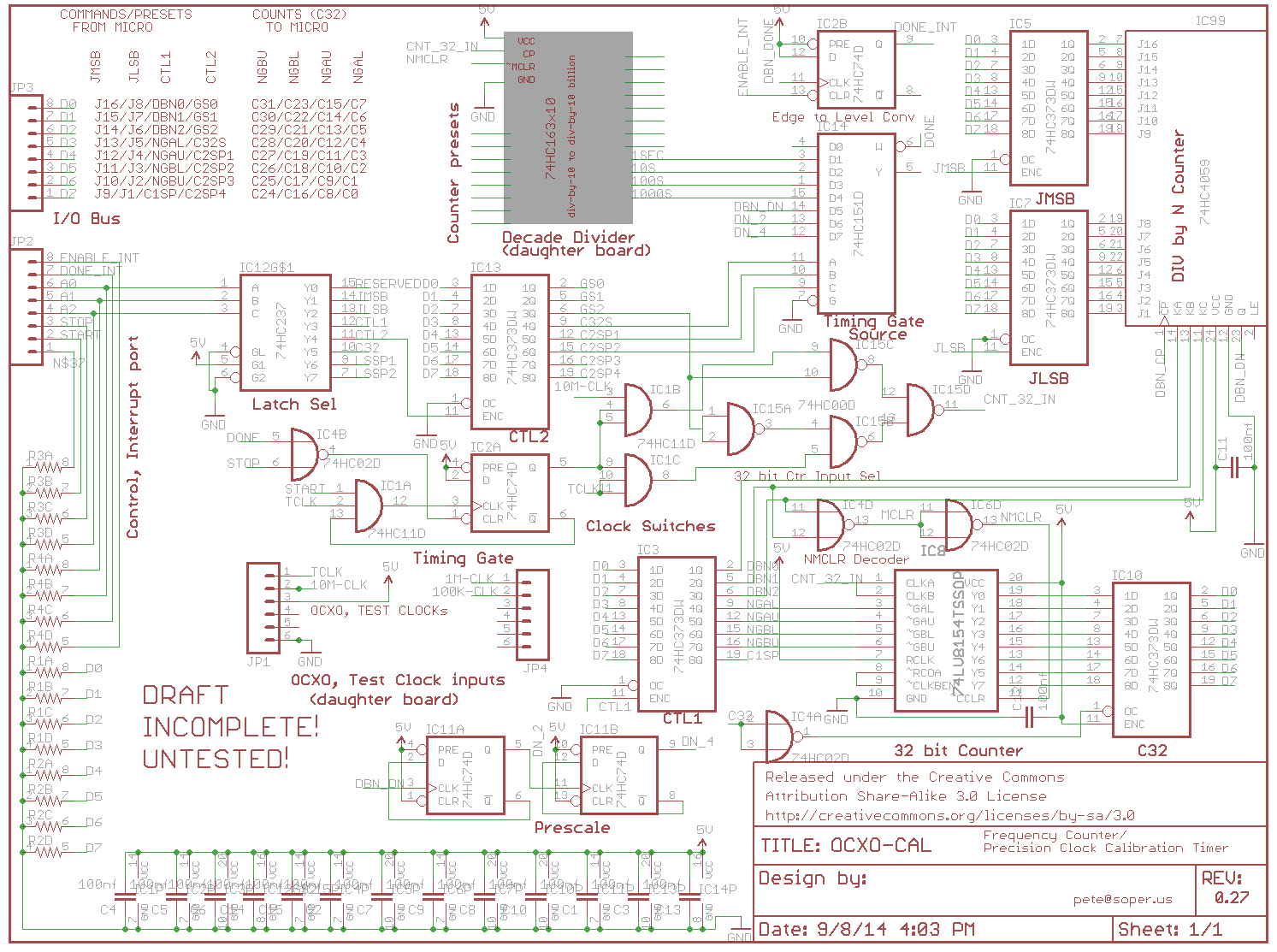
OCXO-CAL 0.24
Well, this is close to mortifying. How I could have read the 74hc4017 datasheet and gotten the impression this chip is effectively like five 74hc390s in one package is a mystery I may never solve. Suffice it to say the delusion is over (the 4017 is a trivial, single decade counter that I could imagine driving somebody’s oxymoronic idea of a “modern nixie tube”. I can’t get back to this immediately but the next schematic will just show some magic signals coming from elsewhere to generate different timing intervals from the OCXO clock. So I’ve now officially spilled the one circuit off this schematic (and one big breadboard).
I split the clock divider/timebase circuit out to a separate daughter board. Except I realized this can also provide the “divide by N” count in place of the 4059. By shifting preset values into a set of registers a set of zeros will result in the OCXO clock being divided down to create timing intervals while nonzero values can be counted (while OCXO clock pulses are accumulated in the 32 bit counter) for the clock calibration function.
But I’m in the middle of tearing up my basement to install a fume hood for the reflow oven and can’t take this further for another few days. But here are the three pieces of the system and these are mostly consistent with each other. But “real soon now” the divider will be made much more flexible and the 4059 and its two ‘373 latches will go away. But, in addition to this I realize while this is being debugged with a solderless breadboard in the picture the precision clock has to be divided down to 1mhz or less. As it was, the 10mhz clock from the LTC chip was bouncing the ground terribly, even with about 20 bypass caps, lower impedance supply and ground paths, etc.
Now on separate pages are the OCXO reference clock and power supply circuit and the time base and down-counter.
So now I’m turning attention back to the main board below, which needs for the gray rectangle to reflect the time base, getting rid of the 4059, etc.
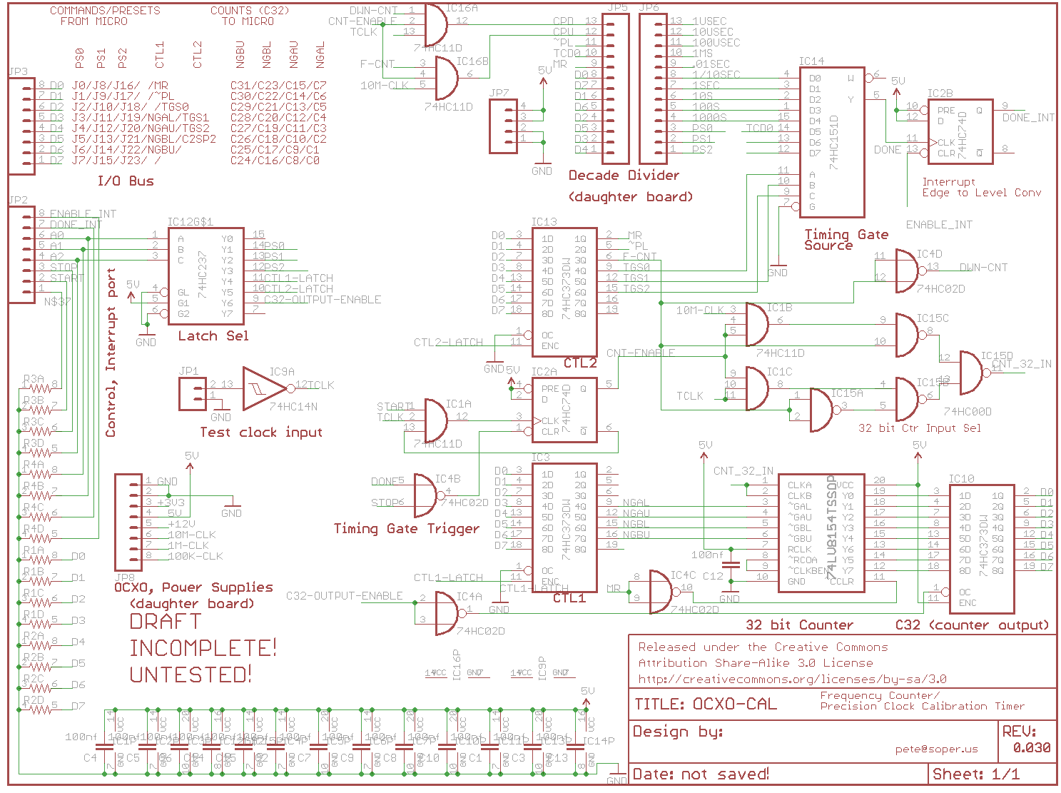
OCXO-CAL 0.27
OK, here’s an update of the main circuit representing the reference clock/power supply daughter board and time base divider/down counter daughter board connections. (Voice from the future: these are links to finished boards) There are many detail errors here, the consistency of naming is non-existent, etc. But here’s where I’m planting a flag. Now while I wait for the rest of the parts to build the clock/PS boards that are in hand and keep reminding myself to order a solder paste stencil for the divider/down counter board at the fab I’m turning attention to how I want to control this system. And of course many readers may be marveling at the small mountain of untested assumptions that have built up. What could go wrong?
OCXO-CAL 0.30
Controlling this thing
In theory to control this calibrator circuit I just need this:
- Eight GPIO pins that can be inputs or outputs
- Six GPIO pins that are outputs
- One GPIO line that can trigger an interrupt. (but actually it could just be polled)
It does seem critical to be able to write all the six output GPIO pins (or at least an essential subset) in a single operation and it isn’t clear what kind of glitches might appear on the 74HC237 decoder chip in any case. There may need to be an extra layer there to keep the rest of the circuit going bonkers as it obediently responds to nanosecond long signal edges.
So, how to run this thing? I don’t intend to use an Arduino sketch. 🙂
I’m thinking about a macro assembler creating a hex file that can drive an interpreter.
Alternatively, a C program with a static local array initialized with a bunch of preprocessor expressions that drive an interpreter.
I really, really don’t want to do something ad hoc.
On the other hand, determining whether the very first assumption about how the logic actually works vs what I think it will do is going to be ad hoc.
But here’s how I think this thing will work:
The control/interrupt port will be divided into six command bits, one input interrupt bit, and one spare. From this point on the six command bits will be called CMD and the interrupt bit will be INT.
The CMD word has six bits:
- Bit 0 – Enable Interrupt
- Bit 1 (skipping over the input bit for the time being) – Latch decoder address A0
- Bit 2 – Latch decoder address A1
- Bit 3 – Latch decoder address A2
- Bit 4 – Stop bit for timing gate trigger
- Bit 5 – Start bit for timing gate trigger
All but the latch decoder bits are individual, while A0-A2 cause the I/O bus (covered below) to be routed to/from some portion of the circuit. So it’s obvious the very next version of the schematic should have A0-A2 in the low order bits and the interrupt input “at the top”, with the unassigned line in between.
The A0-A2 bits are treated as a three bit value from 0-7 and whe these values are are asserted (1=logic high) the effect is as follows:
- 0 – Undefined (by design: when the port driving these pins is all “low” I want it to be a NOP)
- 1 – PS0 – Preset zero. The eight I/O lines are latched into the 74HC373 providing the first two BCD digits of preset values for the chain of 74HC192 decade counters on the down counter daughter board.
- 2 – PS1 – Preset one. The eight I/O lines are latched into the 74HC373 providing the second two BCD digits of preset values for the chain of 74HC192 decade counters on the down counter daughter board.
- 3 – PS2 – Preset twp. The eight I/O lines are latched into the 74HC373 providing the final two BCD digits of preset values for the chain of 74HC192 decade counters on the down counter daughter board.
- 4 – CTL1 – Control One. The eight I/O lines are latched into the 74HC373 driving these control lines:
- 0 – MR – the 74HC192 divider/down counter chain and the 74LV8154 binary counters are reset to zero when this bit is high
- 1 – ~PL – This is an ACTIVE LOW line that is ordinarily high (one). When low the six decimal digits of counter preset values in the decade divider/down counter are loaded into the first three 74HC192 chips to initialize a down count value. When the down count input is pulsed high this preset value is reduced by one and when it underflows with a down count past a zero value the daughter board’s “TCD0” line is asserted to indicate the down counting is completed.
- 2 – F_CNT – When true/high “frequency counting mode” is selected and when false/low “down counting mode” is selected. In frequency counting mode the external test clock input (buffered as signal “TCLK”) is fed into the 32 bit counter while until the end of a selected time base period. When F_CNT is low a preset down count is decremented by the test clock while the (ordinarily 10mhz) reference clock count is accumulated in the 32 bit counter.
- 3 – TGS0 – low order bit of the timing gate source mux
- 4 – TGS1
- 5 – TGS2 – These three mux bits determine whether one of the time base lines or the down counter completion (i.e. TCD0) signals the end of a measurement. The assignments of TGS0-2 are as follows:
- 0 – Timing proceeds until 1/10 second has elapsed (but not really: it’s one million up-count (CPU) pulses and as I write this I realize there need to be jumpers from the OCXO board and a generic label replacing “10M-CLK” because it has to be 1mhz or 100khz during debug with my cheapo breadboard. So this is really “one million CPU pulses”. CPU DOES NOT MEAN CENTRAL PROCESSING UNIT, IT MEANS CLOCK UP.
- 1 – 10 million CPU pulses (ordinarily one second)
- 2 – 100 million CPU pulses (10 seconds)
- 3 – 1 billion CPU pulses (100 seconds)
- 4 – 10 billion CPU pulses (1000 seconds)
- 5 – Timing proceeds until a down count is is finished. That is, all the daughter board CPD pulses are sent until the 74HC192 counter chain underflows. (I’m 99{13079d06258ef9010cea88dee32f3cdfc6f216a54651010f7303ce6140ee927c} sure this means the preset count has to be one less than natural, e.g. a preset of 1 underflows after two down counts)
- 6-7 – Unused
- 6-7 CLT1 values are unused
- 5 CMD value latches the I/O bus lines into the CTL2 latch and these bits are as follows:
- 0-2 Unused
- 3 – the 32 bit 74LV8154 counter “A half” low order byte put into the c32 counter output latch
- 4 – 32 bit counter A-half high order byte is put into the latch
- 5 – B-half low order byte is put into the latch
- 6 – B-half high order byte is put into the latch
- 7 – Unused
- 6 CMD value causes the 32 bit counter output latch (C32) to be enabled to drive the I/O bus. It is IMPERATIVE that the microcontroller configure the I/O bus to “input” before this command value is used.
OK, that’s the whole nine yards. Next is some kind of “language” to express the sequence of operations to do some frequency measurement or precision timing of a test clock input.