(OK, I say tomatoe; my wife says tomahto. But out of respect, we don’t say we use Lienix, or Pythone, right? Although it took from 1991 to the late 90s, we did eventually stop saying Lienix, Leenix and Linooks.)
Chris Gammell, the expert interviewer half of The Amp Hour and long time KiCad supporter, organized a fantastic first KiCon conference in Chicago. Chris conducted some execellent interviews, including one of some of the KiCad developers, including project lead Wayne Stambaugh. Wayne is now employed full time to develop KiCad, a new milestone for this tool that seems to be on track to become the gcc of PCB CAD in coming years.
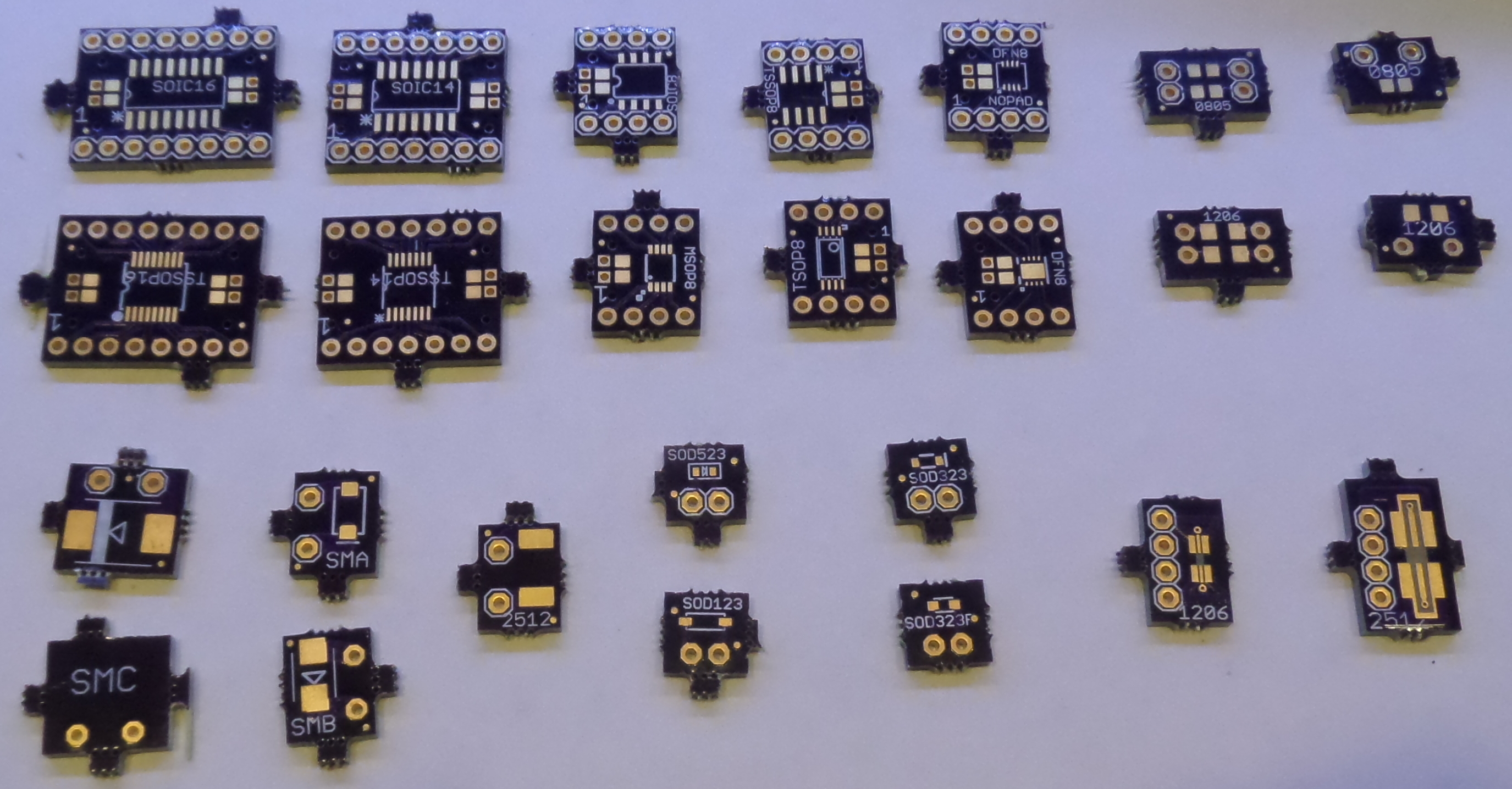
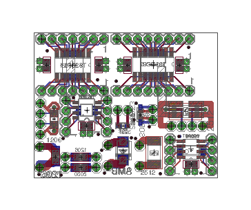
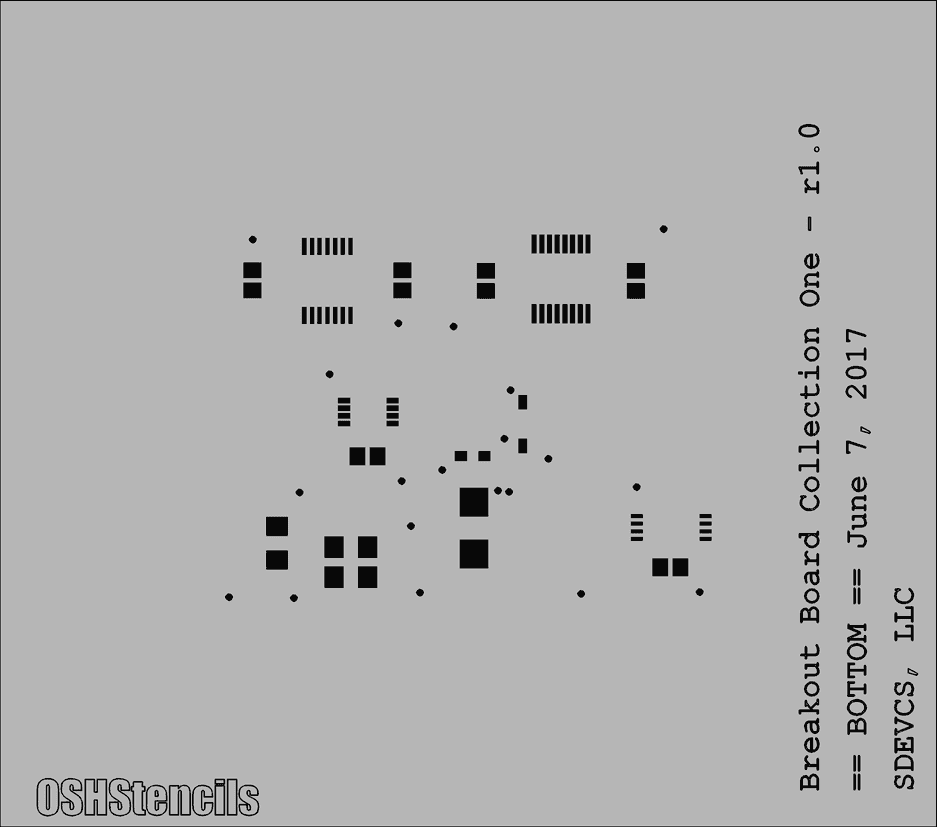
SMD Breakout Board CollectionAggregation of 12 PCB boards for stencil production
As mentioned at the June 12th meeting, I find myself frequently wanting to find the sweet spot for quickly throwing a circuit together to see that gross behavior is as expected and confirm my assumptions correct and the devices perform as advertised before going to the trouble of making a PCB that is likely to be wrong if I’m in too much of a hurry.
But I sometimes find use of SMDs painful with solderless breadboards. First is the headache of having a parallel set of through-hole parts for bread boarding convenience. And of course this is an illusion in many cases: there are no through-hole equivalents for a growing number of components these days. Some shortfalls are obvious, like the current crop of tiny DC conversion chips that seem to be exploring the outer limits of how small a flat pack, no lead package can get. But others are chronic and might be surprising to some readers. Just try finding through-hole versions of some of the specific thermistor types specified for use with things like battery charger chips. It also gets old quick to have to buy a resistor with the same precision value in both through-hole and surface mount packages. And is that through-hole diode slapped on really behaving the same as the specific SMD spec’d for the “real implementation?”
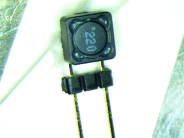
I’ve been accumulating little breakout boards as carriers for various SMDs to make this easier, but that often involves a compromise, such as putting a tiny diode between two SOT-23 pads on a breakout that eats up six pins on a breadboard vs two. Other parts are more challenging and lead to semi-monstrosities like this one for a 22uH inductor:
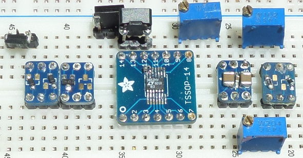
This is what a typical ad hoc collection of parts looks like:
Collection of mostly SMDs on a breadboard
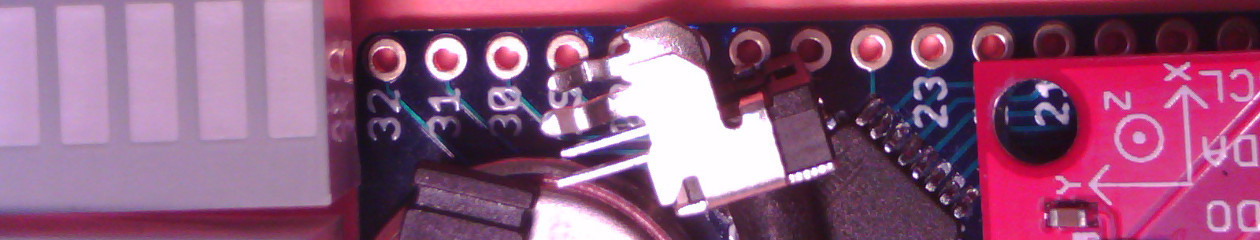
Notice the MSOP12 device is kludged onto a TSSOP14 breakout board. Also notice the (boost) capacitor soldered to the upper left pin of the MSOP12 package in the middle. It’s the barely noticeable bump on pin 12 of the IC (coincidentally below “12”, but electrically connected to header pin “14”, thus the error-prone kludge).
So, although my current breakout collection handles more than 30 devices directly, there are many gaps. This current project will bring the “package coverage” up around the 50 mark, but I estimate I’m only about half done before my hankering for this kind of support mostly dies down. For instance, there would be a lot to gain from handling the common form factors of small switches and connectors, small aluminum electrolytic caps, inductors, transistors, etc. Heck, there’s even real value in making an adaptor that saves me severely abusing a breadboard by cramming TO220 devices into the holes!
Adafruit and SparkFun and others provide some excellent breakout boards at affordable prices (in contrast to Schmartboard’s stuff, which seem to be both too much and too little for my needs). Notice all five of the boards above are Adafruit ones. I have several TI breakout types as well as others. But the actual coverage of package types for the available boards out there is too sparse.
The aggregate PCB rendering above shows the approach I’m taking to build out my collection. This is a collection of 12 PCBs supporting 21 package types that I pulled together for the purpose of making stainless steel stencils. Some of the boards for larger parts have nearby pads for a few passives to make it less painful to handle bypass caps, boost caps, etc, where short connection paths are important.
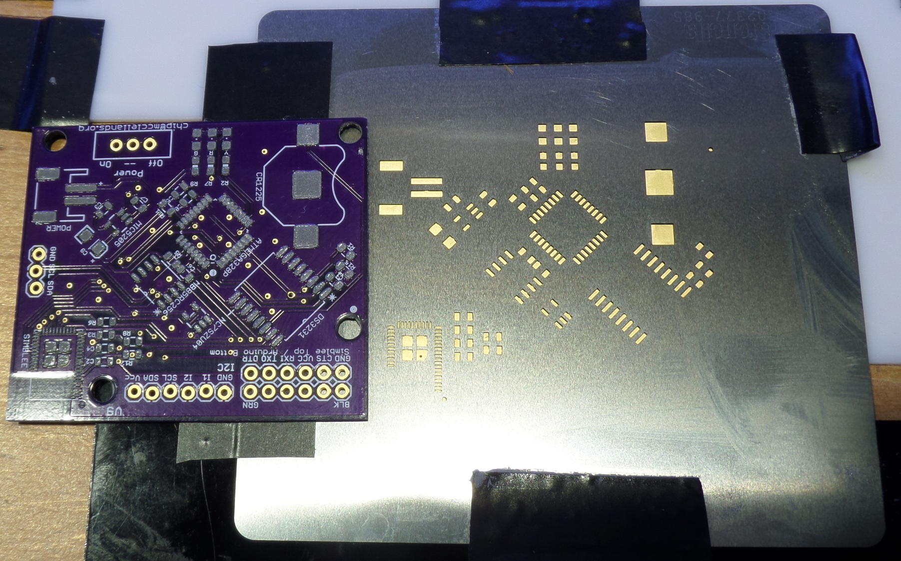
The 12 separate designs (and two others) were sent off to OSH Park to get three copies of each design as a small PCB so I can prove out the breakout boards .
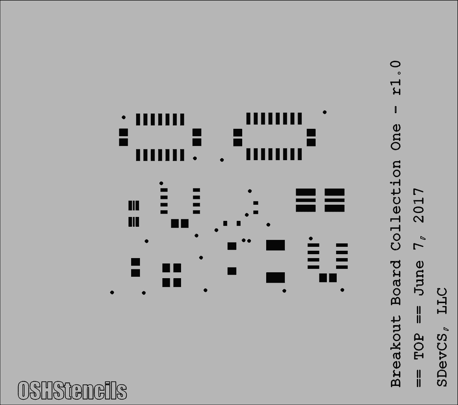
Here is what the stencils from OSH Stencils look like for the top and bottom of the “aggregate PCB”:
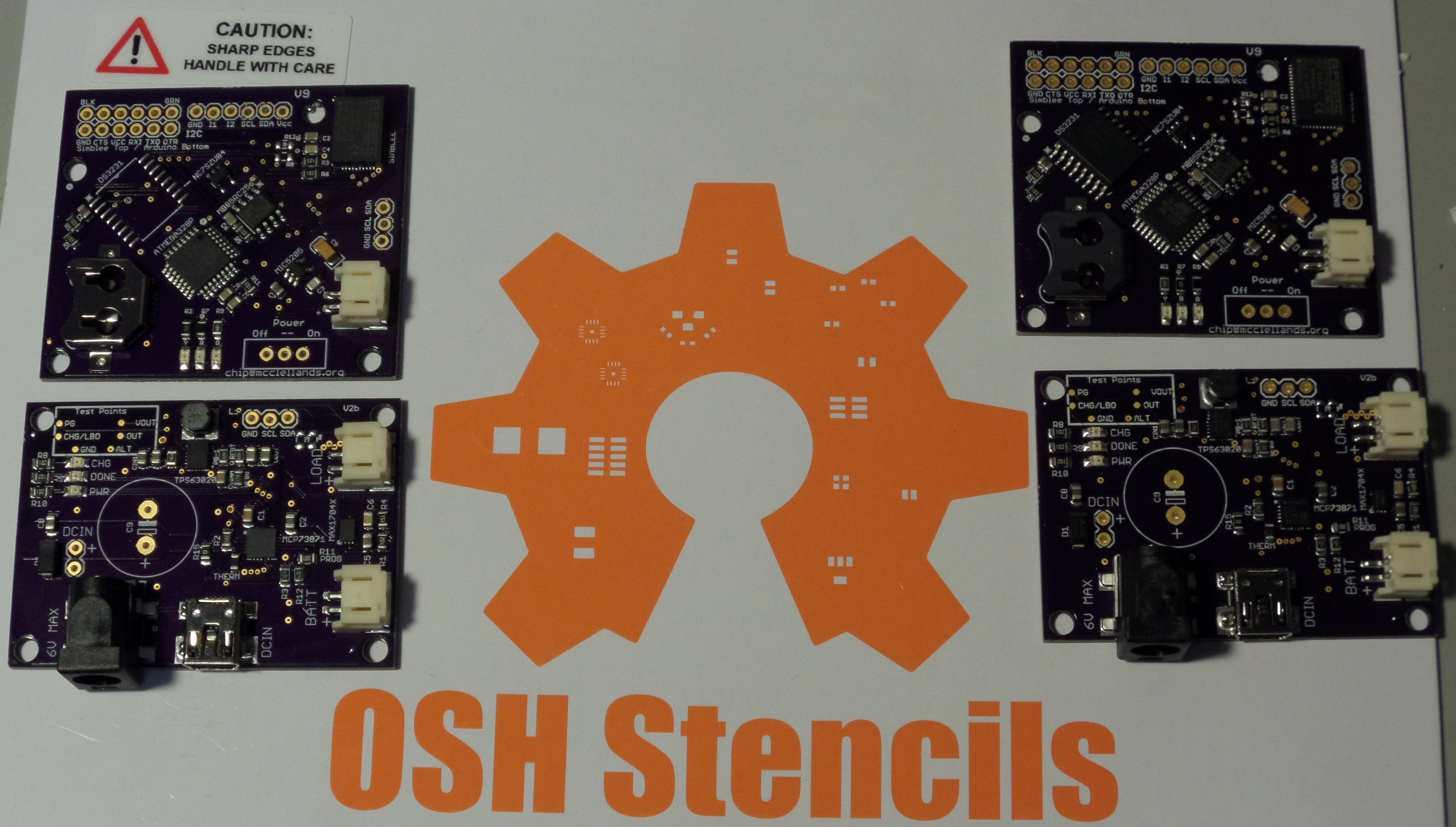
In theory, the work flow is to put the stencil over a particular breakout (e.g. the one for the SOIC14 package in the upper left corner of the top stencil). The one breakout PCB for the package is captured by a holder made of two acrylic “L” pieces vinyl-taped to a dead flat surface. A small squeegee (small piece of plastic credit card) is used to paste over the site(s) for a particular board, then parts are placed and hot air or reflow oven soldering is used.
A quick side note about frames. In many commercial environments the stencil is mounted in a surrounding frame that in turn fits into a jig allowing for rapid handling of boards while maintaining precise registration. I was confused Monday: OSH Stencils is only beta testing frame support with two sizes (relative to these boards those sizes are “wow”, and “my lawn is smaller than that”). Contact them for details if you’re interested.
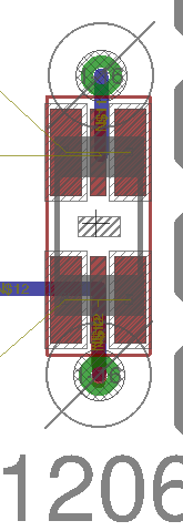
I should also point out that I didn’t spend a lot of time routing these boards. For example, I’ve already had second thoughts about the sense line routes for the two shunt resistor boards that have ‘kelvin connections’ to special middle pads under the resistor ends. Also, as I mentioned Monday, I didn’t spend a lot of time checking things like length to width ratios for some stencil apertures. So the very narrow pad for the 1206 shunt board is technically smaller than the minimum supported size listed for the paste being used (Kester EP256), and the result may be that I can’t actually get paste into this spot properly. The footprint is blown up in the image below. The middle of each set of three pads is .28 millimeters wide. The resistor that sits on these pads is about an eighth of an inch long (yes, king size in relation to how these things are trending).
OK, but how much do those stencils cost? The minimum is $10, but the incremental cost beyond this is less than a dollar a square inch. The two stencils above came to around $22. First class postage with tracking adds $2.75 to an order. My order was completed on a Thursday and I had the stencils in hand the following Monday. With minimal (.75in) borders, everything you see in the first picture above added less than a dollar to each stencil cost. Note that in most cases you’ll only have a stencil for SMDs on one side.
(Update June 22nd)
The first batch of PCBs came back from OSH Park and are shown in the picture at the top of this posting. The tabs sticking out are cut off and squared off with sand paper before the boards are used.
Finally, it’s important to note that some circuits will not cooperate with solderless breadboards and any arrangement of surface mount parts involving long connection paths. Apart from huge amounts of stray inductive and capacitive reactance in the circuit paths, the current carrying limits of breadboards are very real, as is the ability of a simple breakout board to shed heat compared to a PCB having copper pours and other design features to properly handle it.
Planning to offer 1.6mm jigs to eliminate the error vis a visa common PCB thickness (hurray)
For those that didn’t know:
Offering high quality Kester solder paste (in checkout cart, as with the jigs)
Offering stainless steel as well as kapton (stainless steel are common 4mil thickness).
5x5mil smallest feature size possible with kapton stencils. Minimum feature size for steel stencils is ONE MIL!
They see 70/30{13079d06258ef9010cea88dee32f3cdfc6f216a54651010f7303ce6140ee927c} split between 3mil and 5mil thickness of kapton. The 3mil is best for ordinary work, while the 5mil is appropriate for high power devices with large thermal pads, etc. where a lot of solder is needed. I can vouch for the fact that 5mil is a total disaster for fine pitch parts like a QFN package. Kapton in 4mil is unobtanium, which is why they don’t offer that thickness.
Name is OSH Stencils because Brent was originally going to collaborate with Laen of OSH Park, but a change in Laen’s circumstances caused them to remain separate entities and Laen was totally OK with the similarity of names.
Can reduce kapton stencil curl by “counter-rolling” the material and this will give temporary relief.
Started with hobby laser: That “exploded” the first week after starting business. Switched to Epilog 24 (roughly $30k)
Stainless steel stencils made with approx $300k LPKF fiber-based “flagship model” laser cutter
Have maintained 24 hour turn time from the beginning. They went with high end laser to be able to make *the best* stainless steel stencils. They are competitive by avoiding framed stencils and using a proprietary material loading system into the LPKF. Basic cost of framed stencil material is 5X the cost of raw. Could use “pneumatic frame” to simulate real frame, but that didn’t allow sheet sizes that were large enough to be cost effective.
Brent said their charter as they began making steel stencils was to offer the top quality at reasonable prices. He invited people to compare their metal stencils to Chinese stencils under a microscope as they consider potential “cost savings” by going off shore. (OSH Stencils is in the Salt Lake City area of Utah). The metal makeup is different. Most offshore vendors use “inexpensive stainless steel”. Looking at the apertures (the cutouts) you often see grooves to do with the kerf (diameter of laser beam). With low quality metals the edges of apertures have grooves making them look like washboards. Also see minor warping and ripples in the Chinese metal.
Look for “exciting announcements” to do with the stencil process to be offered by OSH Stencils in coming months.
OSH Stencils makes stencils for customers that have nothing to do with electronics. Art projects, special “plates” for mechanical components, etc. They’re open to queries about whether your creative application can be handled by their equipment.
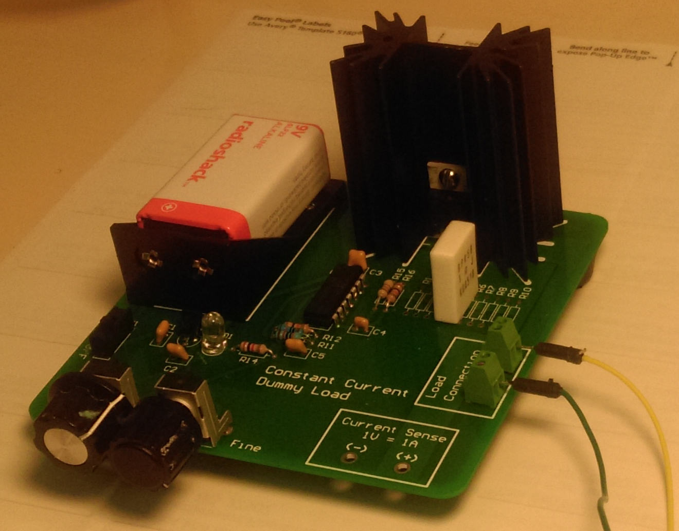
This is a constant current dummy load made from one of Shane Trent’s PCBs like those given away at a recent TriEmbed meeting. As mentioned on the email list, this PCB is a “fixed” version of a design from a “Sleepy Robot” blog of a guy named Wittenberg, which is itself a derivation of an original design by Dave Jones of EEVblog. Wittenberg had made available gerbers for his design (in early 2012) that were unfortunately defective, and he didn’t allow for two way communication, forcing Shane to go to great lengths to correct the gerbers and get a run of PCBs fabricated. Shane’s blog article covers all this in depth and has a link to the corrected gerber files in zip format.
Fast forwarding to the present, here’s a recent tutorial by Dave going into depth about battery measurements. Viewers will just have to put up with the axe-grinding, horse-beating treatment of a “battery life extender” Kickstarter that pushed Dave’s buttons. Apart from this, it’s an excellent treatment and a fantastic “essential subset” spreadsheet tutorial for folks that just want a hint about how to do cool things like the graph-making done in this video.
I assembled and tested a second of the PCBs recently. It will sink up to one amp at up to around the 60 volt limit of the FET used (MTP3055VL) HOWEVER, unless you like to see magic smoke the 18 watt thermal limit of the FET/heatsink assembly has to be honored. So at a full ampere the voltage limit is around 18, and at that load be sure to avoid touching the transistor! At one ampere the shunt resistor will be operating at it’s rated dissipation limit and will also be very hot. To summarize, this load has to be kept at an amp or less and at 18 watts of power dissipation or less. (Note: the shunt resistor is temporarily 5{13079d06258ef9010cea88dee32f3cdfc6f216a54651010f7303ce6140ee927c} tolerance due to an ordering blunder. That will be fixed.)
I’ve decided to make it available for borrowing by TriEmbed meeting attendees who can guarantee it’s return by them or their designee at the following month’s meeting. The transistor is not expensive and it won’t be any big disaster (just embarrassing) if it’s accidentally destroyed, but blowing the traces off the PCB will be frowned upon (joke). So this (and perhaps some of the TriEmbed contact cards Paul made, hallway signs, etc) could be part of a shared resource that could expand over time.
The “UI” is currently two voltmeter test points, with the unit showing the load current as a one to one mapping from amperes to volts. A digital display with simple USB serial (current and “external voltage” aka battery voltage) logging output and some temperature compensation/auto-calibration is planned, but it would be straight forward to tie the test points to something like an Arduino analog pin or two.
Remotely controlling and/or making the current limit programmable would be a bit harder, but a properly coordinated hack to provide an alternative control mechanism would be OK with me and make for a fun project for somebody.
Here are all the design-related links in one place:
The load connection is just four bare plated through holes intended to get some wire loops. These Newark 12H8386 screw terminals solder in and work well.
As mentioned, a momentarily loose screw resulted in this Mouser part 660-MF1/4DCT52R10R0F five watt resistor being substituted for the default 10 1/4 watt resistors. The bad news is this resistor has a 350ppm/C coefficient as well as being only 5{13079d06258ef9010cea88dee32f3cdfc6f216a54651010f7303ce6140ee927c} tolerance. A better choice than either might be a pair of three watt, two ohm 1{13079d06258ef9010cea88dee32f3cdfc6f216a54651010f7303ce6140ee927c} Vishay resistors such as Mouser 71-RS02B2R000FE12. These have 50ppm/C coefficient so there would be about another 1/2{13079d06258ef9010cea88dee32f3cdfc6f216a54651010f7303ce6140ee927c} error at the point you could boil water on them.
I recently added an app to my smart phone and, as a side effect, added another app, and that led me to stumble upon the web site http://everycircuit.com, which provides electronic circuit editing/simulation/presentation tools together with commercial and crowd sourced example circuits.
For those whose religious convictions or practical circumstances make Chrome available on a laptop/desktop, the rest of this page might be interesting. Likewise, if you have a spare $10 the Android or IPhone apps might be interesting. So far, the Android version “just works” on my phone and I personally rate it “Uh, I’ve got to put my socks back on.” Finally reading the site’s terms of use use might be a good idea for some people. I carefully read every word, something I rarely do. But I was relieved to see that the EveryCircuit people (currently) appear to stop short of claiming copyright on crowd sourced circuits.
To check this site out, try this link to the user-submitted rectifier circuit example above inside an instance of the Google Chrome browser on a desktop or laptop computer:
Yes, again, this tool isn’t supported in many, many settings that readers of this blog find themselves in. It’s completely dependent on Chrome. On behalf of the company owning this site (that I just found: I have no connection to it), I’m sorry it isn’t more portable.
By the way: Anybody reading this is welcome to submit their impressions of this or anything else here as comments below. TriEmbed meeting attendees or their online friends (such as in Vermont) are invited to request a blog account if they have interest in adding content to this site via blog postings, additional project pages, etc. Your access will be proportional to how well you’re known to the admins and editors (but we’re always looking for new editors and at least one additional admin!) It takes about 10 minutes with somebody who is WordPress fluent to learn how to add content.
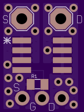
Shane Trent recently shared some recommendations for MOSFET transistors in SOI8 packages that will switch to saturation with ordinary logic level signals. The two transistors he mentions are inexpensive, offer low on resistance, and would seem to be perfect for prototyping, except for one detail. Off the shelf SOIC8 breakout boards such as this one from Adafruit are designed for small signals and modest power supply currents. The N channel part Shane recommends can handle enough current in pulse mode to demonstrate the Adafruit board traces as fusible links. On the other hand, anything beyond a small number of amperes is asking trouble with a breadboard. (For higher power situations Shane’s article also describes interesting transistors in TO220/251 packages.)
After kicking some ideas around a simple breakout board was designed to cover both low-medium and high current use cases. A handful will be coming from OSH Park within the next couple weeks. Here are top and bottom views of the board:
Assuming it has no CAD or fabrication bugs, this board will handle any SOIC8 FET with the pins 1-3 for Source, 4, for gate, and 5-8 for drain. The resistor R1 connects the gate to the source to avoid accidental triggering from high Z or open circuit situations. A value of one megohm should be sufficient. The pads are for an 0805 size resistor. The bottom three pads are for standard or right angle male header pins to go into a standard breadboard. The upper pads are sized for 16 gauge wire to allow high current connections to the source and drain.
Some assembled and bare boards will be brought to the July 13 TriEmbed meeting at NCSU. If the first version is defective we’ll use them to play tiddlywinks. As soon as the board is shown to have no defects the design will be published to the OSH Park “Shared Project” area on their web site.