Category Archives: Device Characterization

Raspberry PI becomes a brand

With the introduction of the Raspberry Pi Pico , “Raspberry Pi” can now be thought of as a brand with two distinct product types. The Pico board features a Foundation-designed chip on a small board only needing header pins, offering an inexpensive but very powerful and versatile microcontroller suited for applications where Linux is less well suited.

With two M0+ Cortex cores, six independent banks of SRAM totaling 254KB, support for execute in place (XIP) from up to 16MB of outboard flash (2MB on the Pico board) at up to 133MHz, and support for variable clock rate and novel programmable I/O control, this is not your everyday low-end Cortex board. Below is a list of links to more details about Pico, its processor chip, firmware, software and tool chain, as well as the complete collection of related source repositories. (1/26/2021: Some host platform-specific tools are also included now. Thanks, Mike Fulbright!).

Raspberry Pi Foundation introduction to Pico

Raspberry Pi Pico specs and list of resources and purchasing sources

GitHub repositories:

micropython
openocd
pico-bootrom
pico-examples
pico-extras
pico-micropython-examples
pico-playground
picoprobe
pico-project-generator
pico-sdk
pico-setup
pico-tflmicro
picotool
thonny-pico

Ubuntu 18.04 Cmake >= 3.12 available from https://apt.kitware.com

Latest ARM crossbuild environment: https://developer.arm.com/tools-and-software/open-source-software/developer-tools/gnu-toolchain/gnu-rm/downloads

Plain Diodes are terrible voltage regulators

Sometimes we’re faced with a situation where a single DC supply is all that’s available but it’s is too much for part of a system and we really wish we had a lower voltage too. I knew diode forward voltage drop is a function of current (and temperature), but I didn’t appreciate just how variable this was until I got lazy and failed to look at a datasheet before I strung some 1N4148 diodes in series as a quick and dirty way to knock 12 volts down to nine. I figured that with the “standard” voltage drop across a silicon junction being .6 volts then 6x.6 = 3.6, and I knew if the current variation gave me around nine volts that would be OK for my application. Except when I tested this I found the variations at the currents the application involved would be all over the map. Here’s a table of what was measured across the six diodes at different values up to the absolute max current for the device:

Forward voltage drop across six 4148 diodes vs current

Here is the same data but for a single diode:

So the per-diode voltage drop is only close to the .6 volts cited for silicon junctions at around one milliampere of current. At the upper current limit of the diodes the drop is very much higher. My application spanned a wide range of currents, so this diode string was hopeless (the client might have noticed a slight behavior change depending on operating mode, and I couldn’t tolerate that.) In my defense over the years I’ve treated diode voltage drops as something I wanted to minimize, making me not just a schottky diode bigot but one who would spend a hour finding the absolute lowest forward voltage drop for a given current. But I obviously developed no intuition at all for the more general cases.

Luckily I found a 7809 linear regulator in my junk box and I can simply carry on without having to order a part, but I thought this might be interesting to share. A high enough power zener would have been another solution.

As mentioned at the beginning, diodes change their behavior with temperature changes too and this is why you sometimes see a diode clamped under or near a power transistor: it’s change in behavior is leveraged with circuitry to keep the transistor from operating outside its safe temperature range. And some folks are able to use tables or perhaps a Taylor series with firmware to monitor voltage drops and use their simple diodes as thermometers.

Battery Testing Resources

LoanerDummyLoad

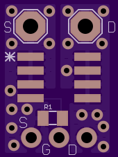
This is a constant current dummy load made from one of  Shane Trent’s  PCBs like those given away at a recent TriEmbed meeting. As mentioned on the  email list,  this PCB is a “fixed” version of a design from a “Sleepy Robot” blog of a guy named Wittenberg, which is itself a derivation of an original design by Dave Jones of EEVblog.  Wittenberg had made available  gerbers for his design (in early 2012)  that were unfortunately defective, and he didn’t allow for two way communication, forcing Shane to go to great lengths to correct the gerbers and get a run of PCBs fabricated. Shane’s blog article covers all this in depth and has a link to the corrected gerber files in zip format.

Fast forwarding to the present, here’s a recent tutorial by Dave going into depth about battery measurements.  Viewers will just have to put up with the axe-grinding, horse-beating treatment of a “battery life extender” Kickstarter that pushed Dave’s buttons. Apart from this, it’s an excellent treatment and a fantastic “essential subset” spreadsheet tutorial for folks that just want a hint about how to do cool things like the graph-making done in this video.

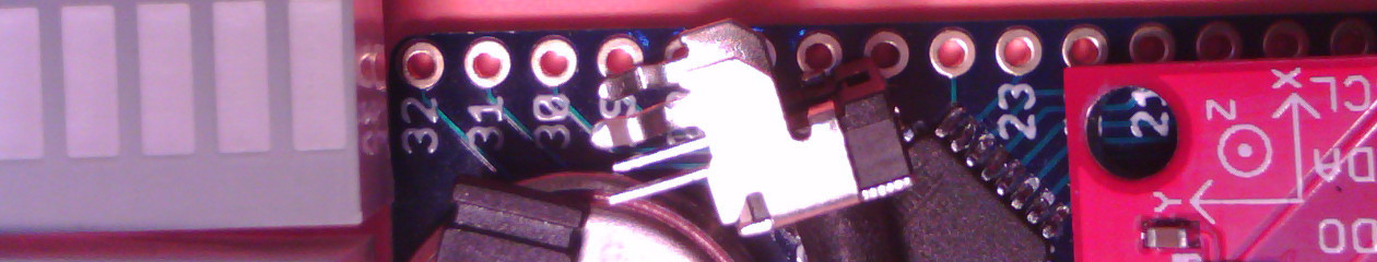
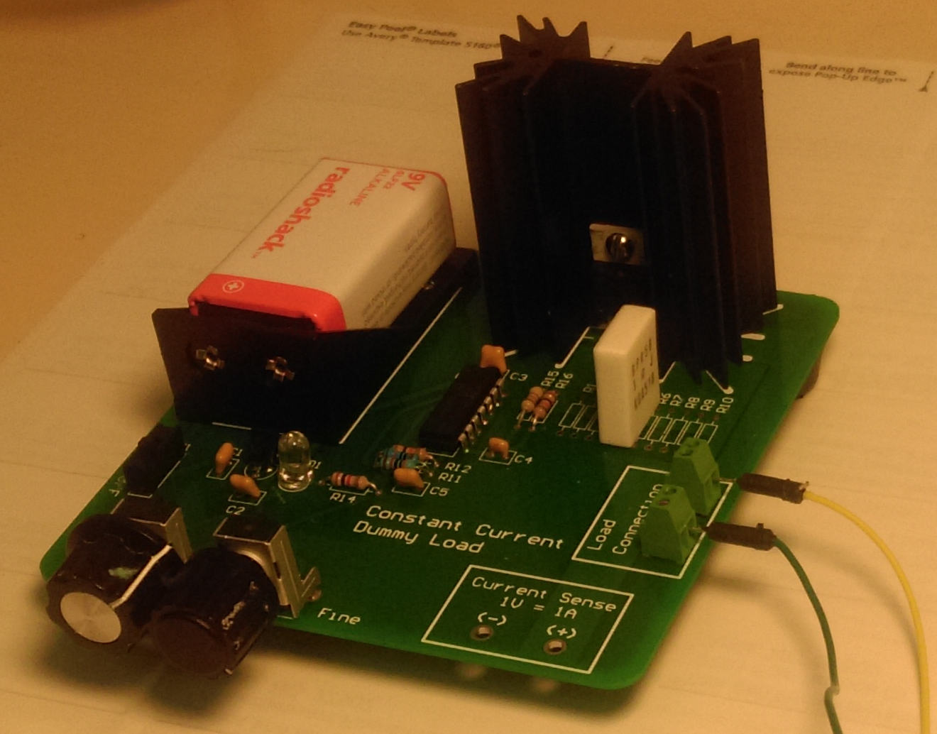
I assembled and tested a second of the PCBs recently.  It will sink up to one amp at up to around the 60 volt limit of the FET used (MTP3055VL) HOWEVER, unless you like to see magic smoke the 18 watt thermal limit of the FET/heatsink assembly has to be honored. So at a full ampere the voltage limit is around 18, and at that load be sure to avoid touching the transistor! At one ampere the shunt resistor will  be operating at it’s rated dissipation limit and will also be very hot. To summarize, this load has to be kept at an amp or less and at 18 watts of power dissipation or less. (Note: the shunt resistor is temporarily 5{13079d06258ef9010cea88dee32f3cdfc6f216a54651010f7303ce6140ee927c} tolerance due to an ordering blunder. That will be fixed.)

I’ve decided to make it available for borrowing by TriEmbed meeting attendees who can guarantee it’s return by them or their designee at the following month’s meeting. The transistor is not expensive and it won’t be any big disaster (just embarrassing)  if it’s accidentally destroyed, but blowing the traces off the PCB will be frowned upon (joke). So this (and perhaps some of the TriEmbed contact cards Paul made, hallway signs, etc) could be part of a shared resource that could expand over time.

The “UI” is currently two voltmeter test points, with the unit showing the load current as a one to one mapping from amperes to volts. A digital display with simple USB serial (current and “external voltage” aka battery voltage)  logging output and some temperature compensation/auto-calibration is planned, but it would be straight forward to tie the test points  to something like an Arduino analog pin or two.

Remotely controlling and/or making  the current limit programmable would be a bit harder, but a properly coordinated hack to provide an alternative control mechanism would be OK with me and make for a fun project for somebody.

Here are all the design-related links in one place:

Here are some BOM changes:

  • The load connection is just four bare plated through holes intended to get some wire loops. These Newark  12H8386  screw terminals solder in and work well.
  • As mentioned, a momentarily loose screw resulted in this Mouser part 660-MF1/4DCT52R10R0F  five watt resistor being substituted for the default 10 1/4 watt resistors. The bad news is this resistor has a 350ppm/C coefficient as well as being only 5{13079d06258ef9010cea88dee32f3cdfc6f216a54651010f7303ce6140ee927c} tolerance.  A better choice than either might be a pair of three watt, two ohm 1{13079d06258ef9010cea88dee32f3cdfc6f216a54651010f7303ce6140ee927c} Vishay resistors such as Mouser 71-RS02B2R000FE12. These have 50ppm/C coefficient so there would be about another 1/2{13079d06258ef9010cea88dee32f3cdfc6f216a54651010f7303ce6140ee927c} error at the point you could boil water on them.

Low Voltage MOSFET Transistors

Shane Trent recently shared some recommendations for MOSFET transistors in SOI8 packages that will switch to saturation with ordinary logic level signals.  The two transistors he mentions are inexpensive, offer low on resistance, and would seem to be perfect for prototyping, except for one detail. Off the shelf SOIC8 breakout boards such as this one from Adafruit are designed for small signals and modest power supply currents. The N channel part Shane recommends can handle enough current in pulse mode to demonstrate the Adafruit board traces as fusible links. On the other hand, anything beyond a small number of amperes is asking trouble with a breadboard. (For higher power situations Shane’s article also describes interesting transistors in TO220/251 packages.)

After kicking some ideas around a simple breakout board was designed to cover both low-medium and high current use cases. A handful will be coming from OSH Park within the next couple weeks. Here are top and bottom views of the board:

PowerFetSOIC8-1-topPowerFetSOIC8-1-bottom

Assuming it has no CAD or fabrication bugs, this board will handle any SOIC8 FET with the pins 1-3 for Source, 4, for gate, and 5-8 for drain. The resistor R1 connects the gate to the source to avoid accidental triggering from high Z or open circuit situations.  A value of one megohm should be sufficient. The pads are for an 0805 size resistor. The bottom three pads are for standard or right angle male header pins to go into a standard breadboard. The upper pads are sized for 16 gauge wire to allow high current connections to the source and drain.

Some assembled and bare boards will be brought to the July 13 TriEmbed meeting at NCSU. If the first version is defective we’ll use them to play tiddlywinks. As soon as the board is shown to have no defects the design will be published to the OSH Park “Shared Project” area on their web site.


Open standard for connector/wire-free charging adopted by major car manfacturers

Open Dots Compatibility Logo


Ford, Chrysler, RAM, Dodge, and Scion have embraced an open standard for conveniently recharging portable devices that appears to be more effective and just easy to use as inductive charging systems. It’s called Open Dots.

The basic idea is to use a set of four parallel conductive strips to carry positive and negative voltages (or +V and ground, depending on your point of view) and have the package of a device to be charged connect to the charging strip automagically just by resting on it. The device to charge has a pattern of four conductive “dots” on its case that will properly connect with the charging pad in any orientation. This scheme was invented for recharging toys in 1963.

I’m sharing this as a potentially handy way to deal with the general problem of recharging battery-operated gadgets. It would take a fair amount of work to implement the pieces and parts involved with the actual electrical connections, but based on  the specification this is on the other end of the scale from rocket science and one would hope that the basic components may be or become cheaply available if the auto industry is involved .

As far as I can tell from their web site anybody could freely use these circuits and connector specs without consequences. (In order to sell something using the Open Dots logo one would need to execute and abide by a member agreement. But you do not need to get within a mile of this logo and could simply use the specs and reference circuits freely until you start selling a ton of stuff and see an advantage to becoming “official”.)

(Open Dots logo used without permission.)

TI Regrooves the MSP430?

(This is the moral equivalent of a press release that is not based on anything remotely official from TI. I know NOTHING beyond what I’ve read about this subject along with a smattering of MSP430 experience. I’m sharing this because I think it might be of interest to the TriEmbed community.)

Texas Instruments has introduced a new family of microprocessors called the MSP432.  As far as I can tell they’ve combined the very sophisticated power saving modes and mature peripheral functional blocks of the MSP430 family with an ARM M4F core.  I’m writing this because the initial chips are available in a QFP package.

The initial chips come with a couple of generous flash memory/RAM sizes combinations and run at 48mhz. Claimed integer MIPS/MHz are substantially higher than with the MSP430 and current consumption from the datasheet is only 90uA/MHz. But these are probably marketing MIPS and most assuredly marketing microamperes, as they understandably assume little or no peripheral subsystem activity. (Take it from me, you can get any result you want from the Dhrystone benchmark with a good compiler).  Still, to the extent that the MSP430’s programmatic support for low power modes is present in spades with a new “power manager” function, and the fact that the chips come with ROM-code peripheral libraries to make porting from the 430 easier, this seems to be an interesting development. I view this as a smart, if not surprising move by TI.

Additional info:

TI Info page

MSP432P4xx Technical Reference Manual

MSP432P401x Mixed Signal Microcontrollers Data Sheet

Alternative short distance rangefinder: measures light transit time, not reflection angle

Here’s a device available on a pair of Sparkfun boards that Rod pointed us and Triangle Amateur Robotics to:

http://datasheet.octopart.com/VL6180XV0NR-1-STMicroelectronics-datasheet-26529471.pdf

Update from Rod: A sensor + ARM M4 eval board for $20 from the chip maker:

 http://www.mouser.com/ProductDetail/STMicroelectronics/EVALKIT-VL6180X/?qs=sGAEpiMZZMvfpQN6QVmrfGjb{13079d06258ef9010cea88dee32f3cdfc6f216a54651010f7303ce6140ee927c}252b49cDybCa83Lgq8kEXU{13079d06258ef9010cea88dee32f3cdfc6f216a54651010f7303ce6140ee927c}3d