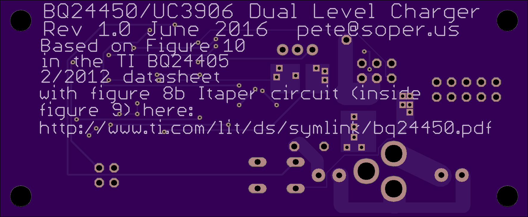
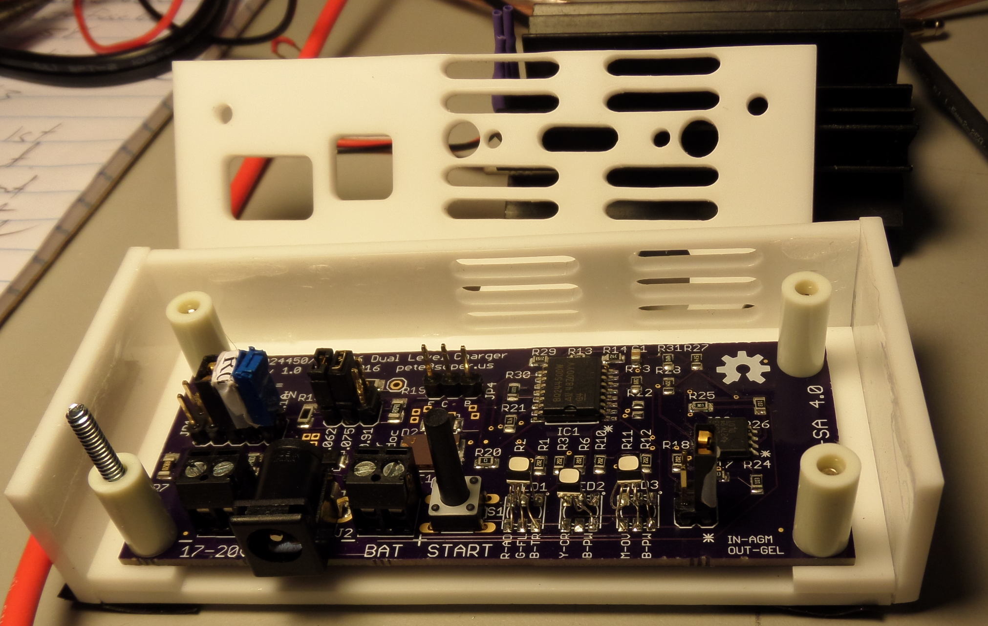
I’ve just sent off for three PCBs from OSH Park for a lead acid battery charger. This is a classic “wheel reinvention” exercise, but I used it as an opportunity to do a deep dive into how the charger chip works as well as many other aspects of lead acid battery charging. It’s not perfect (the trickle current detection could best be described as “funky”), but this will do wonders for the Durham Makerspace sign batteries this fall. The images below are what OSH Park expects the boards to look like. A first cut at a layout for the top of the enclosure and what the enclosure looked like after my first ever laser cutter experience is below the boards. The schematic and Eagle and mechanical files will be on GitHub shortly.
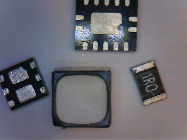
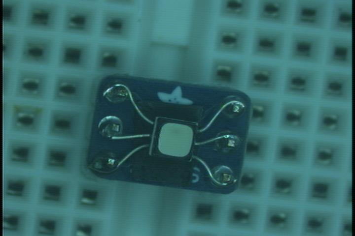
Below is a photograph of the Cree RGB LED used for the display (it will use three of them). It’s smaller than expected (about 1/4 of the size!) I must have been looking at the wrong datasheet, as I thought it was a very standard 5mm square package. That’s an 0805 resistor along side it for scale. I can hand solder these LEDs onto the first prototype boards without any real trouble.
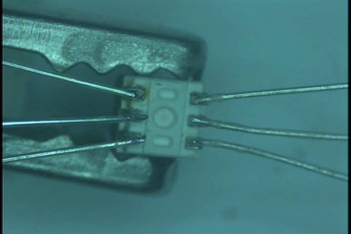
In the meantime, here’s one of the LEDs mounted on a breakout board for testing. With a 19v supply mimicking that of the charger circuit and 2k current limiting resistor each of the three LEDs is BRIGHT. The magenta and yellow combinations look great.
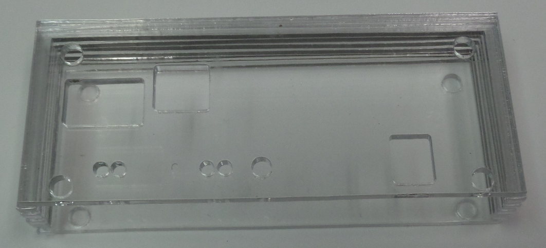
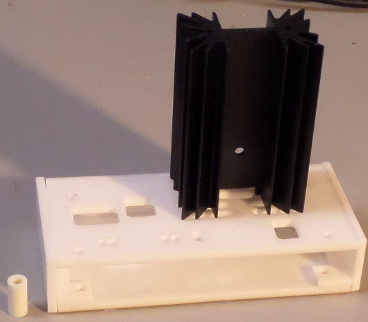
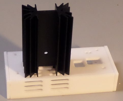
Here’s an updated enclosure laser cut out of white acrylic. The idea would be to relieve the area where the LEDs would shine through. Not sure that’s practical, but this was mostly to explore this layout. The hole for the pass transistor connection is in the wrong place, and the whole thing is too short (the spacers fit exactly, leaving no room for the board!).
The boards came back from OSH Park while was traveling. Here’s an assembled board with kludged on LEDs. I broke the glue joint on the top piece and it’s going to fit back just right with just a tiny height mismatch: perfectly fine for a prototype. I just need proper length screws.
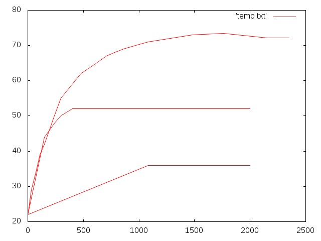
It works! With a 19v (very cheap, plentiful laptop) supply, the heatsink tops out at 50C rise over ambient after 40 minutes at an Imax of 1.5 amps. This is exactly as calculated. Wow, this math/physics stuff actually works. This is of course way too hot to touch the heatsink, but all the parts should stay happy (the TIP147 is practically on vacation with this load). The diodes top out at 32 degree rise and the bq24450 chip temperature rises 14 degrees. All of this is due to heat conduction through the board, as the charger chip is using less than a milliampere total (the base drive of the pass transistor is only 160 microamperes and the divider runs at 49 microamperes, so a milliampere is probably a stretch). More care with the copper pours and positioning of the diodes with the next board should help with this.
Of course with a lower supply voltage the pass transistor heating is going to be way lower (allowing a higher max current).
The Imax jumper settings for 1.5A gives 1.47 amps. Close enough! The Vf (float) of 13.35V is a bit below the design target of 13.5 and the Voc (overcharge/absorption) is 14.3 instead of 14.5V. I was forced to use two 5{13079d06258ef9010cea88dee32f3cdfc6f216a54651010f7303ce6140ee927c} resistors in the part of the divider chain that determines these two voltages, so I’m totally pleased. I should be able to dial these voltages in just right with 1{13079d06258ef9010cea88dee32f3cdfc6f216a54651010f7303ce6140ee927c} resistors.
Now to solder some LEDs on.
Here’s a graph of the temperatures in C vs time in seconds with the 1.5 amp charging and 19v supply described above. From bottom to top the graphs are charger chip, diodes, and heatsink.
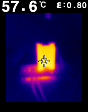
With a 16 volt supply the peak temperature is much lower. Here’s a FLIR 165 picture of the charger during a 1.5A peak charge (exact current not measured: systematic data coming):
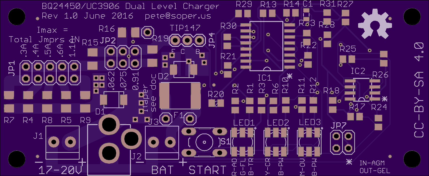
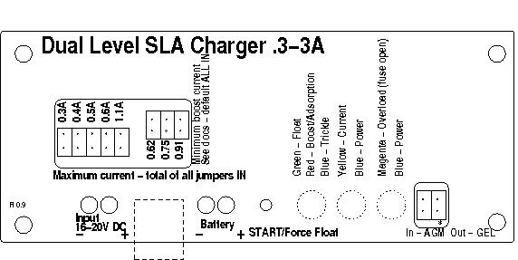
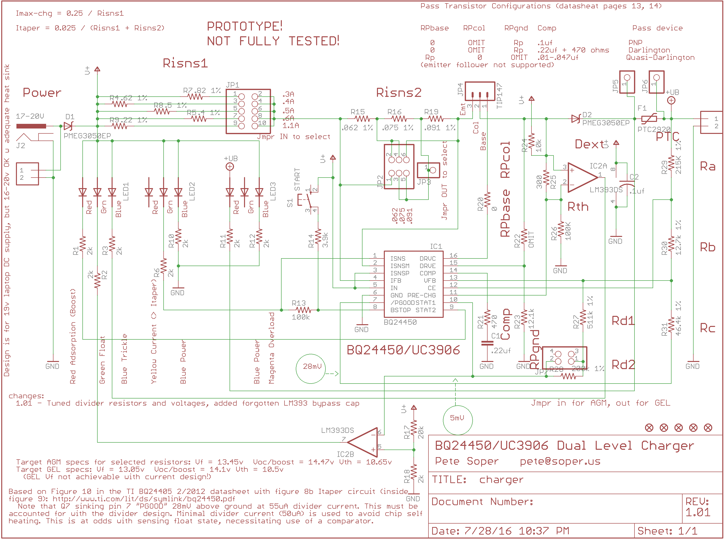
Here is the current schematic. Little caveat: The LED circuitry is completely untested and the colors indicated may not match the schematic text. BIG CAVEAT: The .02 ohm resistance of shorting jumpers in the Risns2 shunt circuit messes up Itaper. The minimum current at the transition from overcharge/boost/absorption to float charge is bound to be wrong because of this, but that hasn’t been measured yet. Other caveat: The “start” switch has been deemed not useful and is going to be replaced with an electronic push on/push off power switch in the next version. As it is “start” has not been tested, but theoretically forces the charger back to it’s initial state.
Design Errors
Here’s a list of mistakes identified so far:
- LED footprint wrong
- Schottky diode silk screen cathode marking on wrong end
- Missing bypass cap for LM393
- LED color combinations ambiguous
- Divider current undershot TI’s recommended 50uA minimum (a couple uA low).
- The choice of divider current has implications for the set of 1{13079d06258ef9010cea88dee32f3cdfc6f216a54651010f7303ce6140ee927c} resistors for a particular choice of Vf, Voc, and Vtrickle (and the two values of Voc for AGM and GEL compatibility), and the current 50uA target choice was completely arbitrary and resulted in a “can’t get there from here” situation with the trickle voltage parameter. Python to the rescue to find the best fit.
- Divider resistor values not quite right due to lacking the right values in 0805 size
- Schottky output diode WAY too close to the PTC fuse, coupling heat into it and causing it to trip at greater than 2.2A Imax. I put provision in for a through hole PTC fuse, however, and think this problem can be avoided with the current board, allowing testing at higher current levels to be finished. As it is, at 2.2A the diodes and fuse will BURN YOUR FINGER during early stages of a charge cycle.
- Copper pours too close to the BQ24450, coupling heat into it (16C rise at 1.5A Imax).
- The tiny Cree RGB LEDs are a cheap, general solution to the wrong problem. Vanilla, 3 or 5mm, through hole LEDs that can sit under the case and generate proper focused spots of color would probably be better. But the cost of this choice is a great deal higher (about $6 vs $1.50 for these Crees). But when all the dust settles it may turn out that a simpler indicator system is acceptable.
- Position of pass transistor connection pads relative to where the heat sink goes conveniently is wrong.
- The PTC “fuse open” LED indication isn’t working.
- The float and boost/absorption (improperly labeled “AD”) LEDs are swapped (i.e. red == float, green == boost). This is probably a second order problem from getting the LED footprints mixed up.
- Ditto for the “current > Itaper” LED being red instead of green (creating magenta when it is on with the always-on blue power LED).
- Assuming red and green are swapped with the third LED, it means the fuse open indication would be cyan instead of magenta.
- The precharge/trickle current (Ipre) came out too low (15mA vs the intended 25) and the trickle threshold voltage (Vth) came out too high (greater than 10.8 volts). But the charger does exactly the right thing when it gets the battery up to Vth, so this just means a deeply discharged battery takes a little while longer to charge.
Here’s a list of technical hazards to finish exploring:
- LED color/brightness levels and “focus” levels as they relate to translucent case materials. At the moment the LEDs shining up into the white acrylic case just create a wide, very diffuse blob of color. Not at all clear how this is going to work.
- Proper functioning of the LM393 for detecting trickle current state was not completely confirmed with the breadboard circuit. Fingers crossed that the low divider current and crazy long wires hanging off the breadboard explain the erratic behavior observed.
Hmm, it appears to be nearly impossible to get a proper photo of the unit with the LEDs shining. Here’s the best so far, overriding all the camera settings possible to keep the LEDs from being a single, amorphous blob of white light.
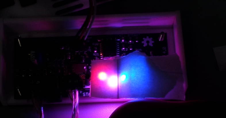
The red and green LEDs are painfully bright (at roughly 7-8mA each). In this shot from left to right the red LED lit shows the charger is in boost/overcharge/absorption mode. Two colors are lit in the middle LED, appearing to be white in this shot but to the eye is very clearly magenta (i.e. “current over Itaper” and “power” both on). The right most LED is the second blue power indicator. The charger is putting 2.1 amps into a battery, pulling the voltage toward Voc.
After a few days with these LEDs the use of “combinations” to convey different charger states is clearly problematic, because the colors are not easily discriminable. It’s becoming a priority to “mix” colors with the LED on the breakout board in order to determine whether more easy to judge colors can be arranged with adjustments to the charger’s current limiting resistors. If not, these nice, cheap, bright Cree LEDs need to be replaced with discrete ones that offer spacial discrimination to avoid ambiguity.
ECO Plan
- LED connections & current limit resistors to get a more reasonable set of indicator colors.
- Try to fix the LM393 circuits, starting with missing bypass cap.
- Replace the SMD fuse with a radial through hole.
Board Respin Plan
- Consider switching the Risns2 shunt to the datasheet “8a” design and add a jumper or two. This would boil down to explicit control of both Imax and Itaper, abolishing the “10{13079d06258ef9010cea88dee32f3cdfc6f216a54651010f7303ce6140ee927c} default” behavior with a (hypothetical) zero Risns2 resistance and the 8b circuit. The fact that the Risns2 value would be the “sum of the jumpers OUT” coupled with the fact that higher Risns2 equates to a lower Itaper will make this charger for thinking people only!!
- Rethink the LM393 kludgefest.
- Fix the copper pours and layout with respect to heat dissipation and heat conduction.
- Start switch -> push on/push off power switch
- Consider right angle headers, right angle power switch, reflector to achieve right angle indicators to move everything to the board edge.
- Consider shifting the Id (voltage comparator divider current) up to 75uA in case this might avoid weird behavior to do with the chip design limits. (Maybe get a question to a TI design engineer about this).
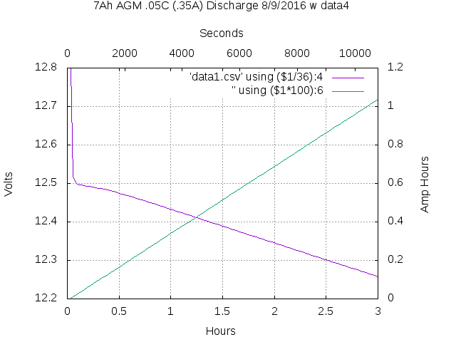
The graph below is a first go with gnuplot output of the data from a Maynuo M9711 electronic load set to draw .35 amps from a 7Ah battery for three hours. The Maynuo will directly generate various file output formats, one being an Excel spreadsheet within the default app for that file type (in this case LibreOffice), allowing easy conversion to a .csv file which can be fed straight into gnuplot.
The hope is that the start/end voltages and slope of the discharge can be used to decipher battery condition and charge levels.
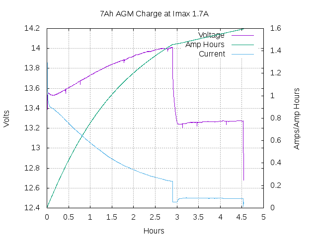
Here’s a charge cycle with the first proto build. The overcharge(aka boost aka absorption) voltage and the float voltage are both set too low. Arranging for the divider behavior to correlate with the datasheet for the bq24450 chip is turning into a pain.
This graph was made with gnuplot from data collected from a Rigol DM3068 using its ethernet interface via a hacked version of an open source Python IVI library.
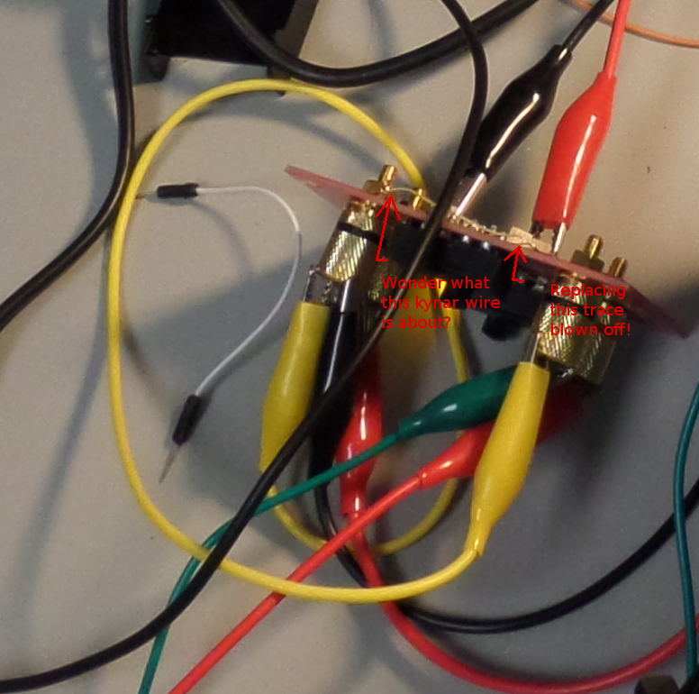
I had earlier fat-fingered the DMM and blown the high current shunt fuse, which is inside the meter behind a warranty seal. After a half hour of phone calls that established that Rigol service is modest with a six point type, lower case “m”, I got a dispensation to open the box and replace the fuse with documentation that will preserve the last 2/3 of the warranty. But in the meantime, while fretting about dropping a bundle on shipment of the meter to/from a service depot, I still needed to log data. What I ended up with was strange, but it worked. I found that the EEVblog uCurrent can be run at higher than 3v power supply voltage (safely to 5.5, I set the limit to 4.5v) and this enables up to +/- a couple amps of precision measurement. So I used that for current measurement with the 3068 by measuring the voltage output of the uCurrent set to a mV/mA. To measure the battery voltage at the same time I had the 3068 measure current through a series resistor around 1k ohms, with a calibration factor in the Python code to precisely translate the 11-odd mA of current to the battery voltage. Strange, but true.
To add terrible insult to injury, I had an accident with the uCurrent, momentarily asking it to pass current between its two “-” terminals. It wasn’t designed for that and I literally blew a trace off the PCB. I soldered a wire on the back of the board and made it a happy camper again. But this is what the board looks like (couldn’t take a microscope picture, but one end of the trace is still curled up for a future photo).
But in the midst of this I broke down and bought a cheap but capable DMM. I’ll do a quick demo with some slides at the September 12th TriEmbed meeting at NCSU and post them to the meeting archive so a relatively complete story will be available.
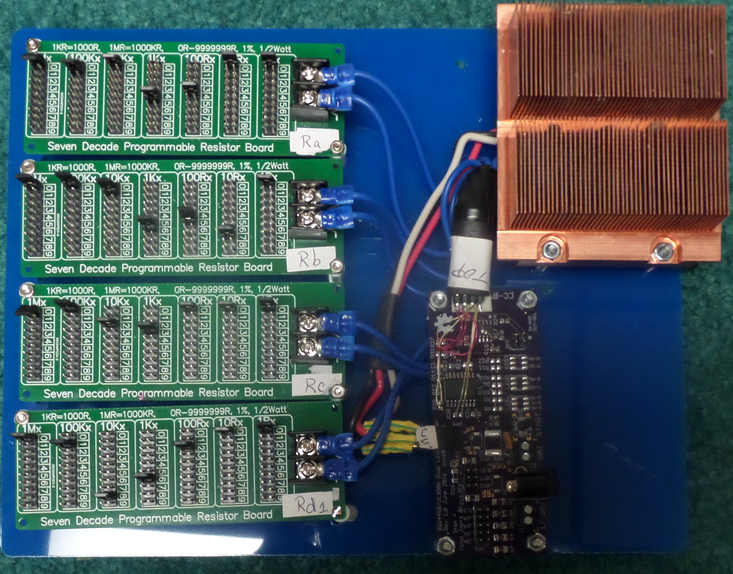
Meanwhile, a second rev1 board was partially populated for more testing. The LEDs and their current limiting resistors were left off, a through hole PTC fuse was substituted for the surface mount to reduce heating by the diodes. A bypass cap was added to the comparator chip and four of the divider circuit resistor pads were wired to a connector to support outboard decade boards. Finally, a very stout connection was made to a pass transistor on a massive, solid copper heat sink. The whole thing was mounted on a laser-cut sheet of acrylic: