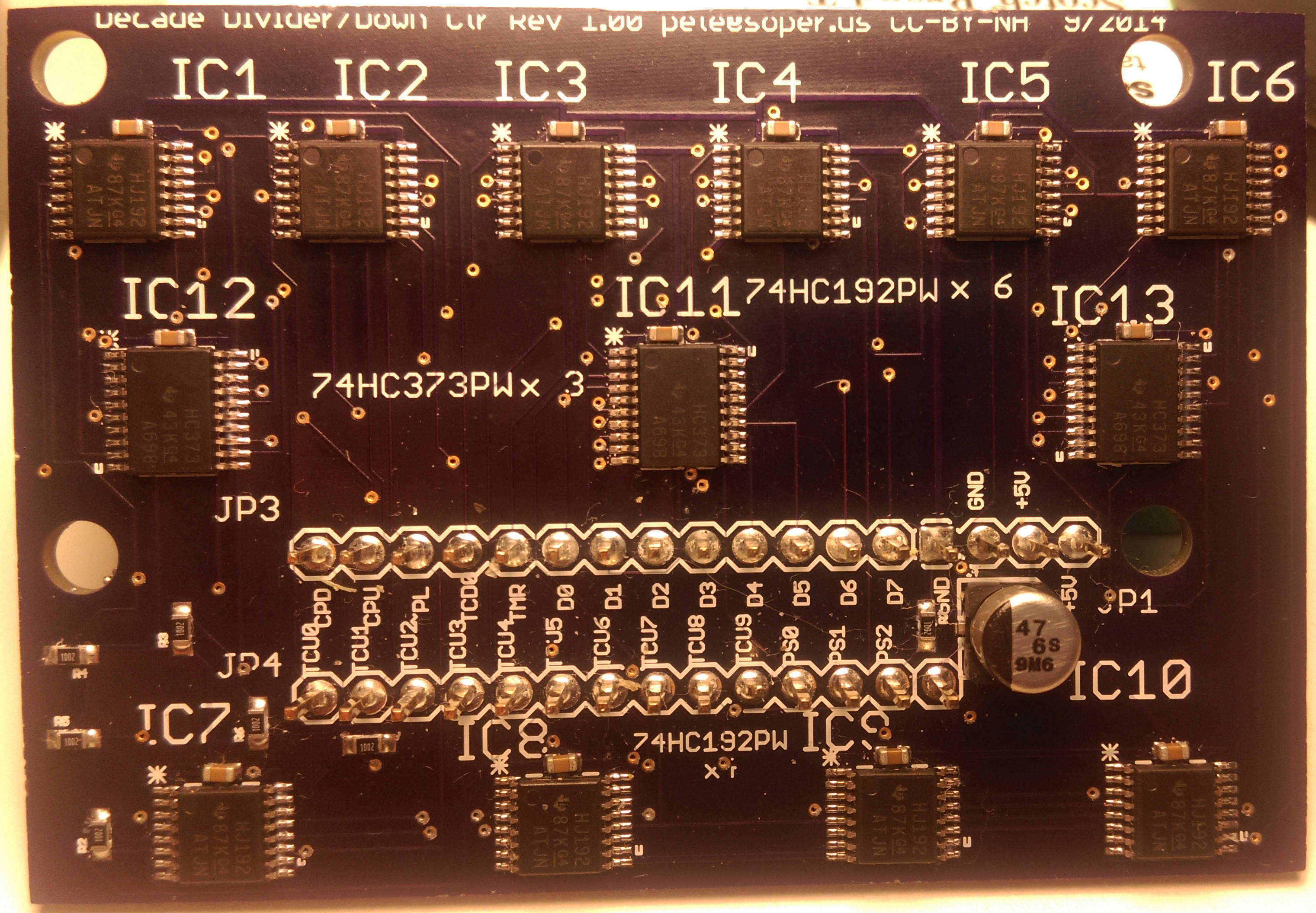
Here’s the second finished piece of the calibrator/frequency counter project: a daughter board that connects to the main logic board.
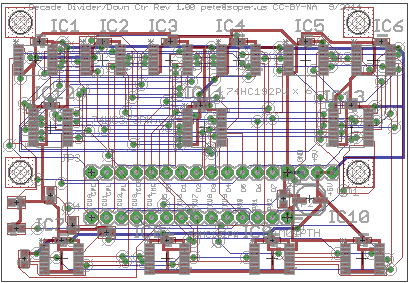
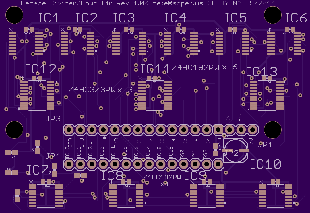
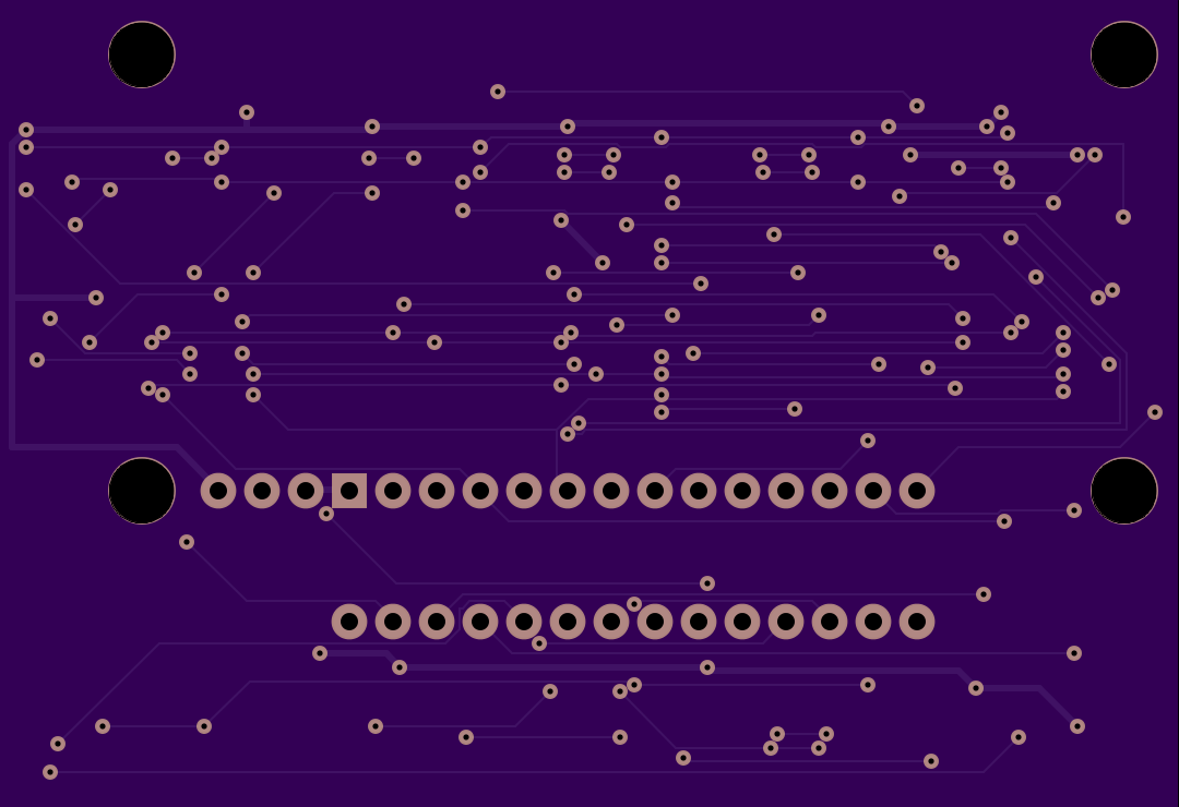
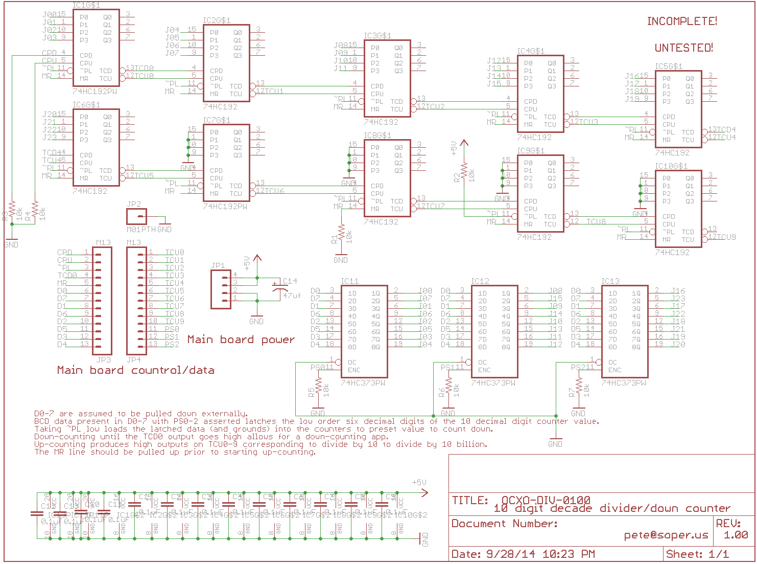
This is a set of 10 74HC192 synchronous presettable decade counters with the first 24 bits (six BCD digits) settable via a set of three 74HC373 latches. The control signals, latch bus, power and ground area all on headers spaced for placement on a solderless breadboard. In fact I’ll be using extra long headers that stick out top and bottom: the two rows of signal lines are arranged to plug directly into a logic analyzer. But the board can also operate on its own mounted on nylon standoffs. If/when there was a need to redo this board a much smaller connector (or merging with surrounding circuitry) would save a lot of board space.
In operation a reference square wave fed into the “up count” input of the first 74HC192 will create a set of successive divide by 10 count outputs that will be used when the calibrator is operated in the familiar “frequency counter” mode. With the eventual 10mhz square wave from the OCXO reference board the divider chain will create time base signals from one microsecond to 1000 seconds. The counters all operate in lock step and advance on the same up count so there is no random ripple delay and the time base edges should be very accurate relative to the input clock. A master reset line is available to get a clean start in up count mode. I presume that without this random high order bits in the counter chips could create very odd behavior for a while.
An alternative , “down count”mode is to put six BCD digits into the three latch chips, pull the parallel load line low, and preset the counters to a starting value. Then a square wave on the “down count” input of the first 74HC192 will count the whole chain downward until the first counter finally underflows, signalling a “borrow” from that digit and the end of the down-count sequence. This function will obviate the need for the separate “divide by N” 74HC4059 counter of the main calibrator circuit (which I’m turning attention back to now).
There are a lot of vias in this board. I played some games with chip placement and latch bus assignments for the sake of getting the via count down to “only” about 140. I checked these “creative pin assignments” at least seven times and want to believe that the fact that the signals go through a consistent path is the key, but if you look at the D0-7 assignments of the latches and the odd arrangment of them wrt to the counter chips you might wonder if I was licking a rural North Carolina frog or something.
I intentionally left out copper pours for the sake of making ECOs easier. Having a ground and/or power plane didn’t make much difference to the via count and having both planes mostly befuddled the routing. The power and ground buses are very fat and I think the bypassing is pretty good, so hopefully the signals will be reasonably clean. But this board represents a huge bet on reality cooperating with theory in several different regards, so we’ll see. This was also done with the Eagle autorouter, but until I played the games described above it wasn’t up to the task.
Most of this work was done in late 2014/early 2015. I’m just getting back to this project now, in March, 2016.
OSH Park’s rendering of the Eagle PCB design:
The schematic:
Eagle board layout: