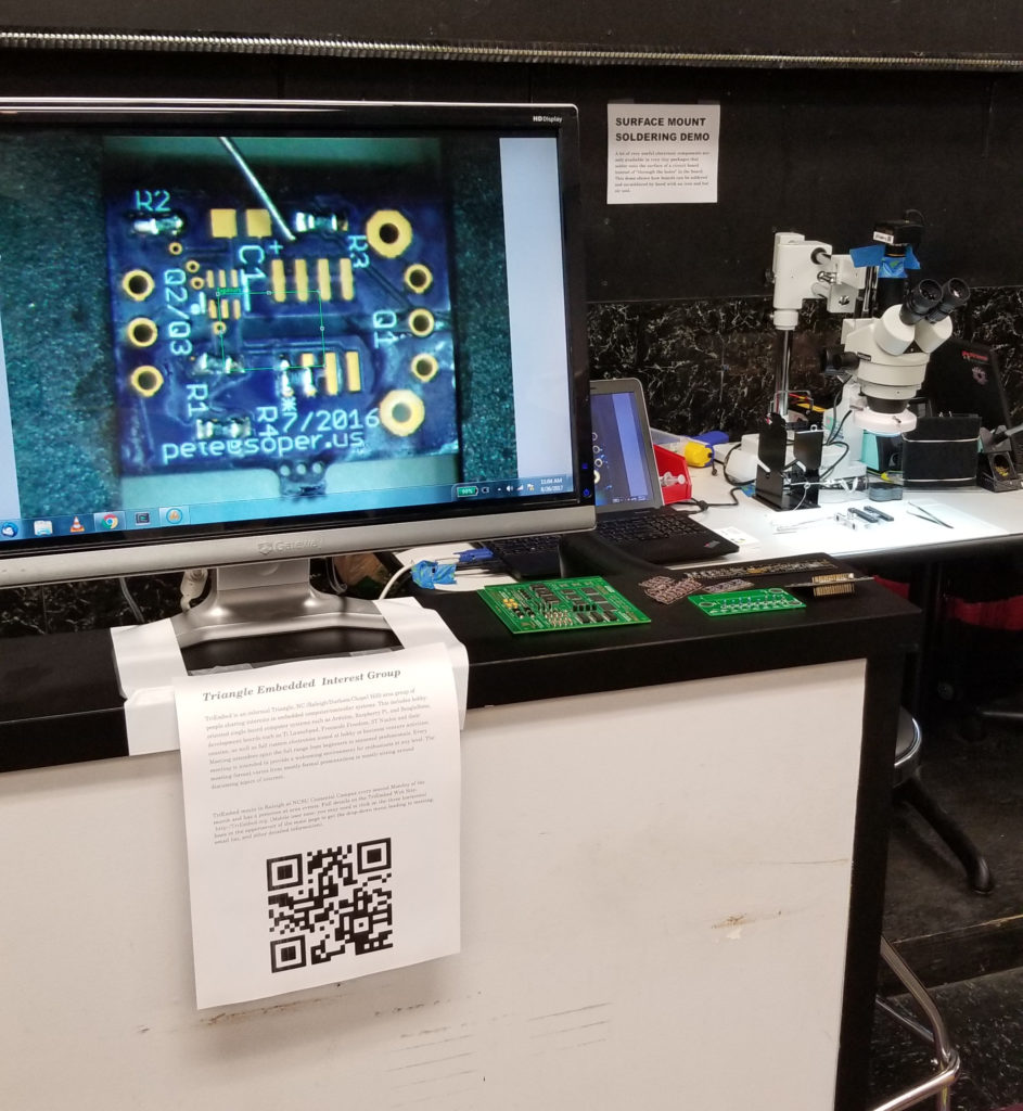
Today until 2pm is the second day of an open house of the area Triangle DIY Biology organization near Scrap Exchange in Durham. I was button-holed to “do something” at this event and decided the easiest thing to demonstrate would be how to hand solder fine pitch SMDs. TriEmbed info sheets are on hand and we’re also plugging SplatSpace. I’m using a little space at the popup to coordinate curation of Fred Ebeling’s Collection of electronic parts at SplatSpace.
All posts by Pete Soper
New from Maniacal Labs: Affordable smart LED support for Raspberry Pi
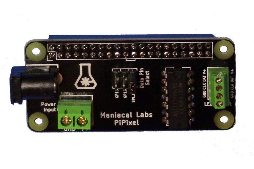
Adam Haile and Dan Ternes of Maniacal Labs have been busy. By accident I came across their site on Tindie and see they have a new product. PiPixel is oriented toward Raspberry Pi enthusiasts who would like to work with smart RGB LED strips. It’s described in detail on their web site. This is a super low cost kit that would make an excellent beginning soldering project with a big payoff. Find all the details on the ‘Labs web site.
OSHPark: Order to shipment elapsed days over 4 1/2 years
Proof of Concepts with SMD Parts
As mentioned at the June 12th meeting, I find myself frequently wanting to find the sweet spot for quickly throwing a circuit together to see that gross behavior is as expected and confirm my assumptions correct and the devices perform as advertised before going to the trouble of making a PCB that is likely to be wrong if I’m in too much of a hurry.
But I sometimes find use of SMDs painful with solderless breadboards. First is the headache of having a parallel set of through-hole parts for bread boarding convenience. And of course this is an illusion in many cases: there are no through-hole equivalents for a growing number of components these days. Some shortfalls are obvious, like the current crop of tiny DC conversion chips that seem to be exploring the outer limits of how small a flat pack, no lead package can get. But others are chronic and might be surprising to some readers. Just try finding through-hole versions of some of the specific thermistor types specified for use with things like battery charger chips. It also gets old quick to have to buy a resistor with the same precision value in both through-hole and surface mount packages. And is that through-hole diode slapped on really behaving the same as the specific SMD spec’d for the “real implementation?”
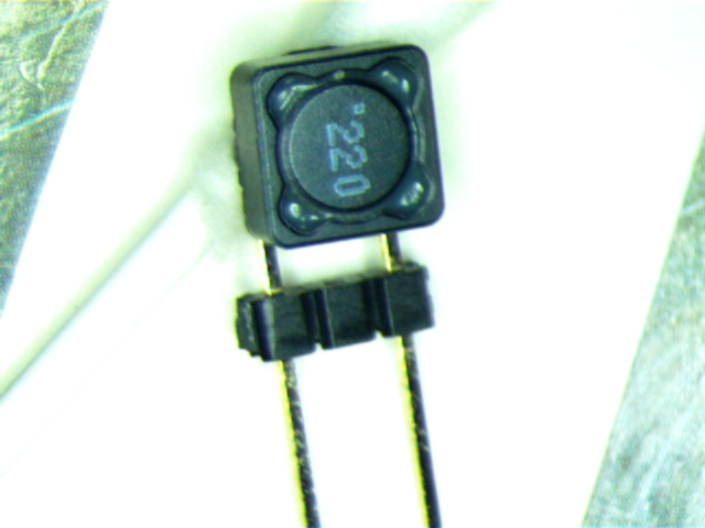
I’ve been accumulating little breakout boards as carriers for various SMDs to make this easier, but that often involves a compromise, such as putting a tiny diode between two SOT-23 pads on a breakout that eats up six pins on a breadboard vs two. Other parts are more challenging and lead to semi-monstrosities like this one for a 22uH inductor:
This is what a typical ad hoc collection of parts looks like:
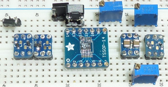
Notice the MSOP12 device is kludged onto a TSSOP14 breakout board. Also notice the (boost) capacitor soldered to the upper left pin of the MSOP12 package in the middle. It’s the barely noticeable bump on pin 12 of the IC (coincidentally below “12”, but electrically connected to header pin “14”, thus the error-prone kludge).
So, although my current breakout collection handles more than 30 devices directly, there are many gaps. This current project will bring the “package coverage” up around the 50 mark, but I estimate I’m only about half done before my hankering for this kind of support mostly dies down. For instance, there would be a lot to gain from handling the common form factors of small switches and connectors, small aluminum electrolytic caps, inductors, transistors, etc. Heck, there’s even real value in making an adaptor that saves me severely abusing a breadboard by cramming TO220 devices into the holes!
Adafruit and SparkFun and others provide some excellent breakout boards at affordable prices (in contrast to Schmartboard’s stuff, which seem to be both too much and too little for my needs). Notice all five of the boards above are Adafruit ones. I have several TI breakout types as well as others. But the actual coverage of package types for the available boards out there is too sparse.
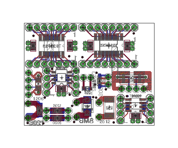
The aggregate PCB rendering above shows the approach I’m taking to build out my collection. This is a collection of 12 PCBs supporting 21 package types that I pulled together for the purpose of making stainless steel stencils. Some of the boards for larger parts have nearby pads for a few passives to make it less painful to handle bypass caps, boost caps, etc, where short connection paths are important.
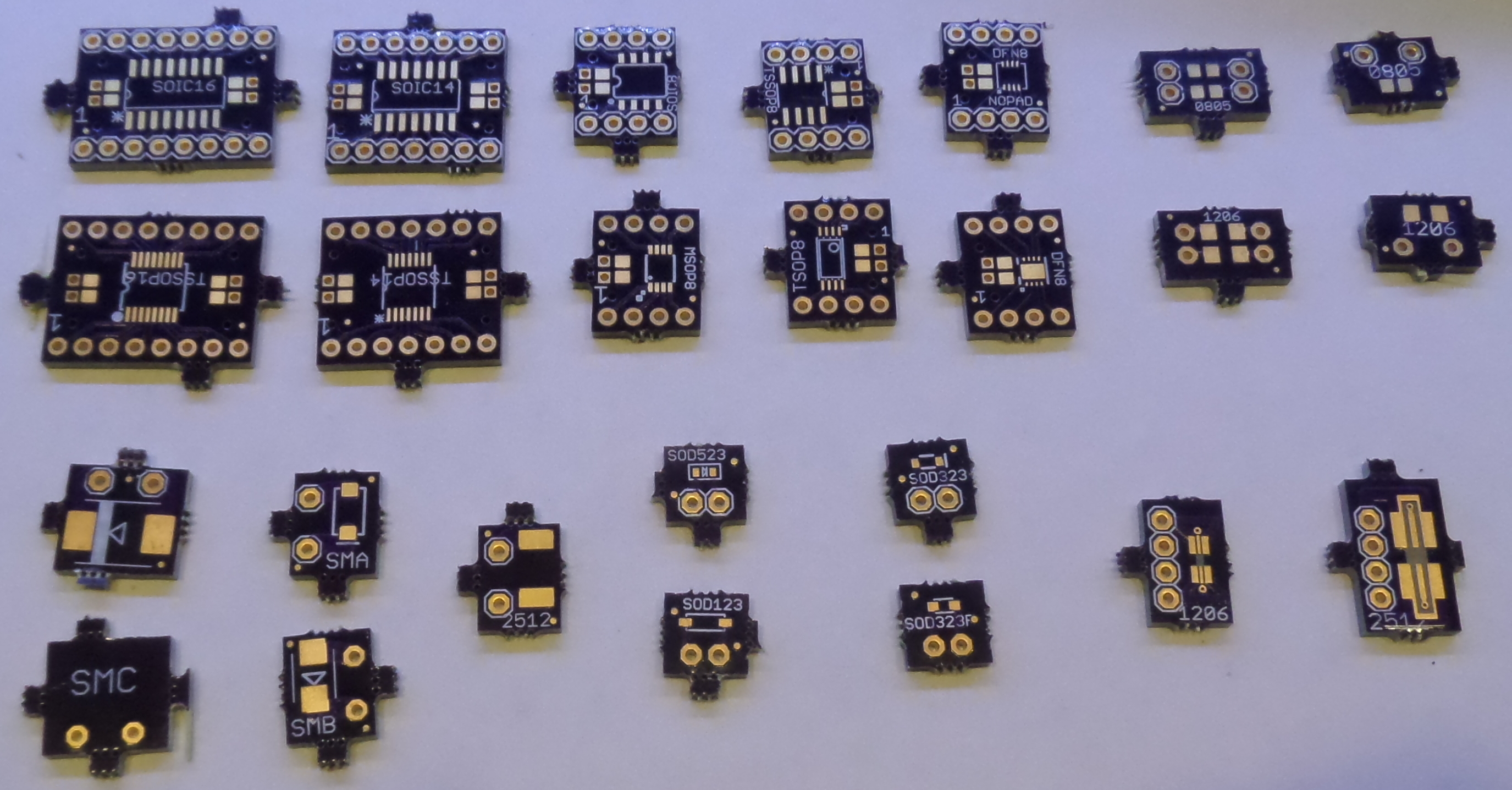
The 12 separate designs (and two others) were sent off to OSH Park to get three copies of each design as a small PCB so I can prove out the breakout boards .
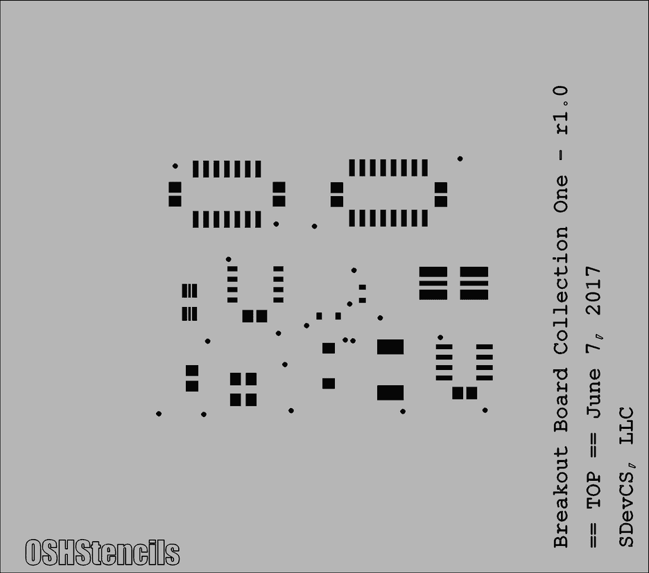
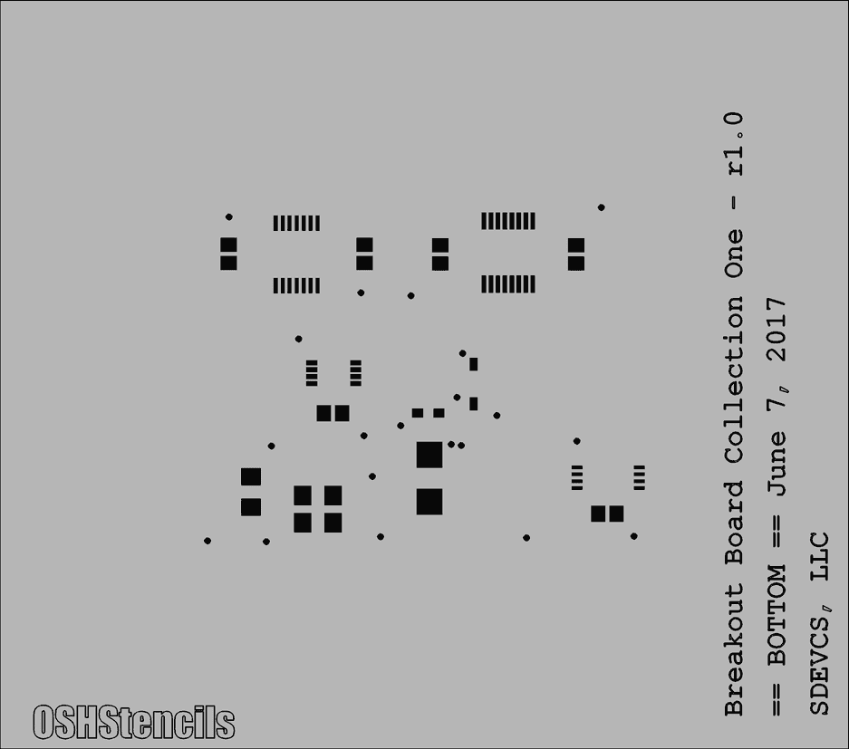
Here is what the stencils from OSH Stencils look like for the top and bottom of the “aggregate PCB”:
In theory, the work flow is to put the stencil over a particular breakout (e.g. the one for the SOIC14 package in the upper left corner of the top stencil). The one breakout PCB for the package is captured by a holder made of two acrylic “L” pieces vinyl-taped to a dead flat surface. A small squeegee (small piece of plastic credit card) is used to paste over the site(s) for a particular board, then parts are placed and hot air or reflow oven soldering is used.
A quick side note about frames. In many commercial environments the stencil is mounted in a surrounding frame that in turn fits into a jig allowing for rapid handling of boards while maintaining precise registration. I was confused Monday: OSH Stencils is only beta testing frame support with two sizes (relative to these boards those sizes are “wow”, and “my lawn is smaller than that”). Contact them for details if you’re interested.
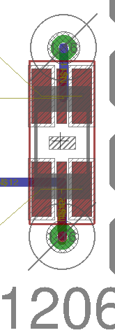
I should also point out that I didn’t spend a lot of time routing these boards. For example, I’ve already had second thoughts about the sense line routes for the two shunt resistor boards that have ‘kelvin connections’ to special middle pads under the resistor ends. Also, as I mentioned Monday, I didn’t spend a lot of time checking things like length to width ratios for some stencil apertures. So the very narrow pad for the 1206 shunt board is technically smaller than the minimum supported size listed for the paste being used (Kester EP256), and the result may be that I can’t actually get paste into this spot properly. The footprint is blown up in the image below. The middle of each set of three pads is .28 millimeters wide. The resistor that sits on these pads is about an eighth of an inch long (yes, king size in relation to how these things are trending).
OK, but how much do those stencils cost? The minimum is $10, but the incremental cost beyond this is less than a dollar a square inch. The two stencils above came to around $22. First class postage with tracking adds $2.75 to an order. My order was completed on a Thursday and I had the stencils in hand the following Monday. With minimal (.75in) borders, everything you see in the first picture above added less than a dollar to each stencil cost. Note that in most cases you’ll only have a stencil for SMDs on one side.
(Update June 22nd)
The first batch of PCBs came back from OSH Park and are shown in the picture at the top of this posting. The tabs sticking out are cut off and squared off with sand paper before the boards are used.
Finally, it’s important to note that some circuits will not cooperate with solderless breadboards and any arrangement of surface mount parts involving long connection paths. Apart from huge amounts of stray inductive and capacitive reactance in the circuit paths, the current carrying limits of breadboards are very real, as is the ability of a simple breakout board to shed heat compared to a PCB having copper pours and other design features to properly handle it.
PCB Board Cleaning: Pure Isopropyl vs MG Cleaner
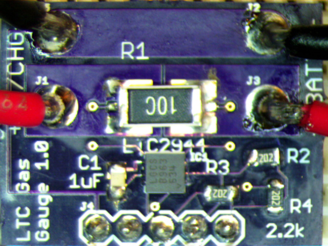
Here’s a breakout board that got a lot of hand soldering with three different kinds of flux. Plain 91{13079d06258ef9010cea88dee32f3cdfc6f216a54651010f7303ce6140ee927c} isopropyl was used after rework using AIM 280 “no clean” (the watery stuff), which, if used copiously, definitely needs cleaning if you care about appearance. In this case, even scrubbing with a nice (Adafruit) ESD-safe brush would not remove the flux completely as can be seen with this first picture below. The gray cast that’s most pronounced in the lower right corner shows this “can’t clean” flux layer:
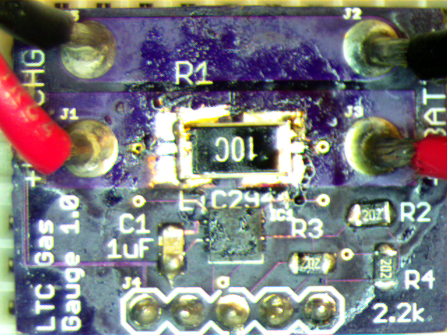
Several rework episodes later, the board had seen lots of the NC flux, but also Chipquik SMD 291 “Tack Flux N/C”, which, in my experience, is never “no clean” except perhaps in the sense of “the electrical connections won’t eventually short out with this stuff”. From an aesthetic perspective the layer of goo left behind in many cases is simply not nice. Finally, I got lazy with a brute force desoldering method involving braid and old style rosin flux and that stuff is of course just plain nasty. So here’s the very sad “before” photo after the shunt resistor and other parts had been messed with a few times:
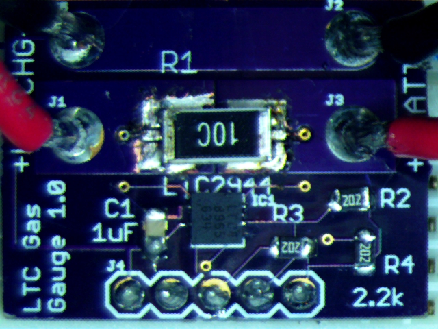
For this case a bit of MG Flux Remover was put into the bottom of a jar, the board was put below the surface, and the jar was swished around for a while. Some exceptionally bad looking, black “baked rosin flux” bits were scrubbed off and then the board got another few seconds in the jar. Then the flux remover was washed off with pure isopropyl to get the “gunk in solution” level down to zero. (This cheap squirt bottle from Rite Aid works very well for this). Then after the board had dried it looked like this:
The result was superb: no gray splodges or any other stains. Notice the very tired traces missing solder mask in places. This is what comes of too vigorous scrubbing. The flux remover looks unchanged and I’m expecting that in the tightly sealed jar it has a lot of use left.
I was expecting the remover to have evil stuff in it and was surprised to find it’s ethanol, isopropyl alcolhol, and ethyl acetate. The latter is found in small quantities in wine (and many homebrew beers). But despite the familiar chemicals I use lots of ventilation for this kind of task.
Thanks to Shane Trent for letting me “try out his jug”.
Notes about OSH Stencils
A few notes from listening to Brent of OSH Stencils: on The Amp Hour:
- Planning to offer 1.6mm jigs to eliminate the error vis a visa common PCB thickness (hurray)
- For those that didn’t know:
- Offering high quality Kester solder paste (in checkout cart, as with the jigs)
- Offering stainless steel as well as kapton (stainless steel are common 4mil thickness).
- 5x5mil smallest feature size possible with kapton stencils. Minimum feature size for steel stencils is ONE MIL!
- They see 70/30{13079d06258ef9010cea88dee32f3cdfc6f216a54651010f7303ce6140ee927c} split between 3mil and 5mil thickness of kapton. The 3mil is best for ordinary work, while the 5mil is appropriate for high power devices with large thermal pads, etc. where a lot of solder is needed. I can vouch for the fact that 5mil is a total disaster for fine pitch parts like a QFN package. Kapton in 4mil is unobtanium, which is why they don’t offer that thickness.
- Name is OSH Stencils because Brent was originally going to collaborate with Laen of OSH Park, but a change in Laen’s circumstances caused them to remain separate entities and Laen was totally OK with the similarity of names.
- Can reduce kapton stencil curl by “counter-rolling” the material and this will give temporary relief.
- Started with hobby laser: That “exploded” the first week after starting business. Switched to Epilog 24 (roughly $30k)
- Stainless steel stencils made with approx $300k LPKF fiber-based “flagship model” laser cutter
- Have maintained 24 hour turn time from the beginning. They went with high end laser to be able to make *the best* stainless steel stencils. They are competitive by avoiding framed stencils and using a proprietary material loading system into the LPKF. Basic cost of framed stencil material is 5X the cost of raw. Could use “pneumatic frame” to simulate real frame, but that didn’t allow sheet sizes that were large enough to be cost effective.
- Brent said their charter as they began making steel stencils was to offer the top quality at reasonable prices. He invited people to compare their metal stencils to Chinese stencils under a microscope as they consider potential “cost savings” by going off shore. (OSH Stencils is in the Salt Lake City area of Utah). The metal makeup is different. Most offshore vendors use “inexpensive stainless steel”. Looking at the apertures (the cutouts) you often see grooves to do with the kerf (diameter of laser beam). With low quality metals the edges of apertures have grooves making them look like washboards. Also see minor warping and ripples in the Chinese metal.
- Look for “exciting announcements” to do with the stencil process to be offered by OSH Stencils in coming months.
- OSH Stencils makes stencils for customers that have nothing to do with electronics. Art projects, special “plates” for mechanical components, etc. They’re open to queries about whether your creative application can be handled by their equipment.
Osh Stencils/Osh Park
Latest Reflow Progress
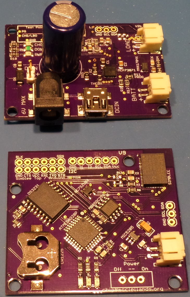
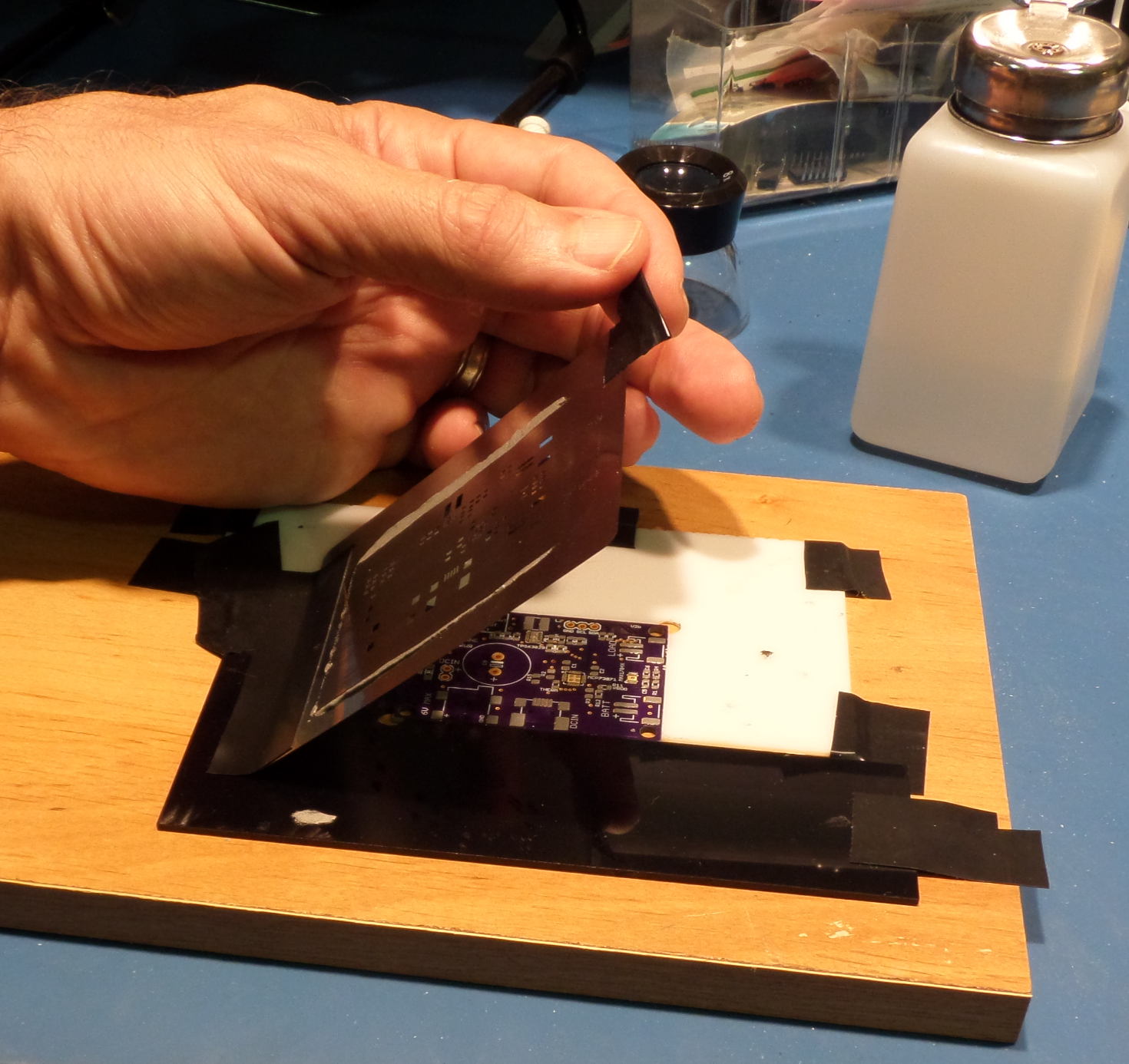
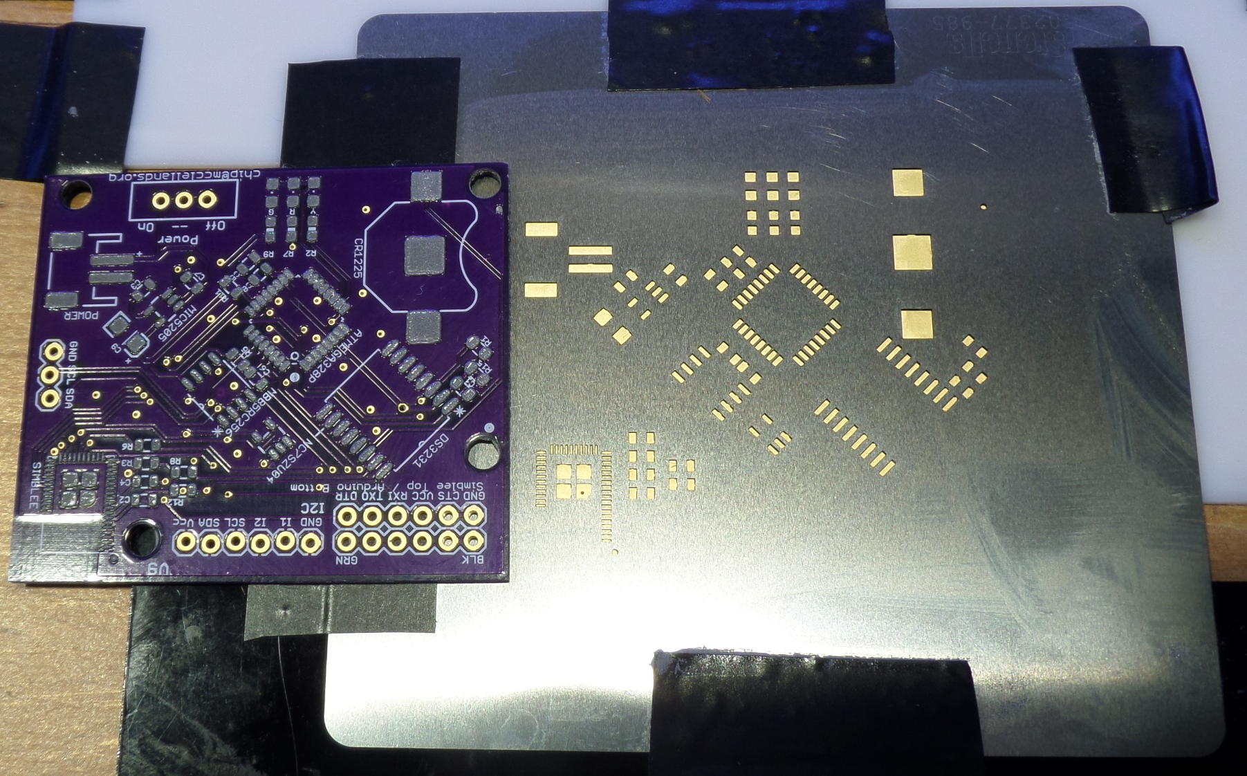
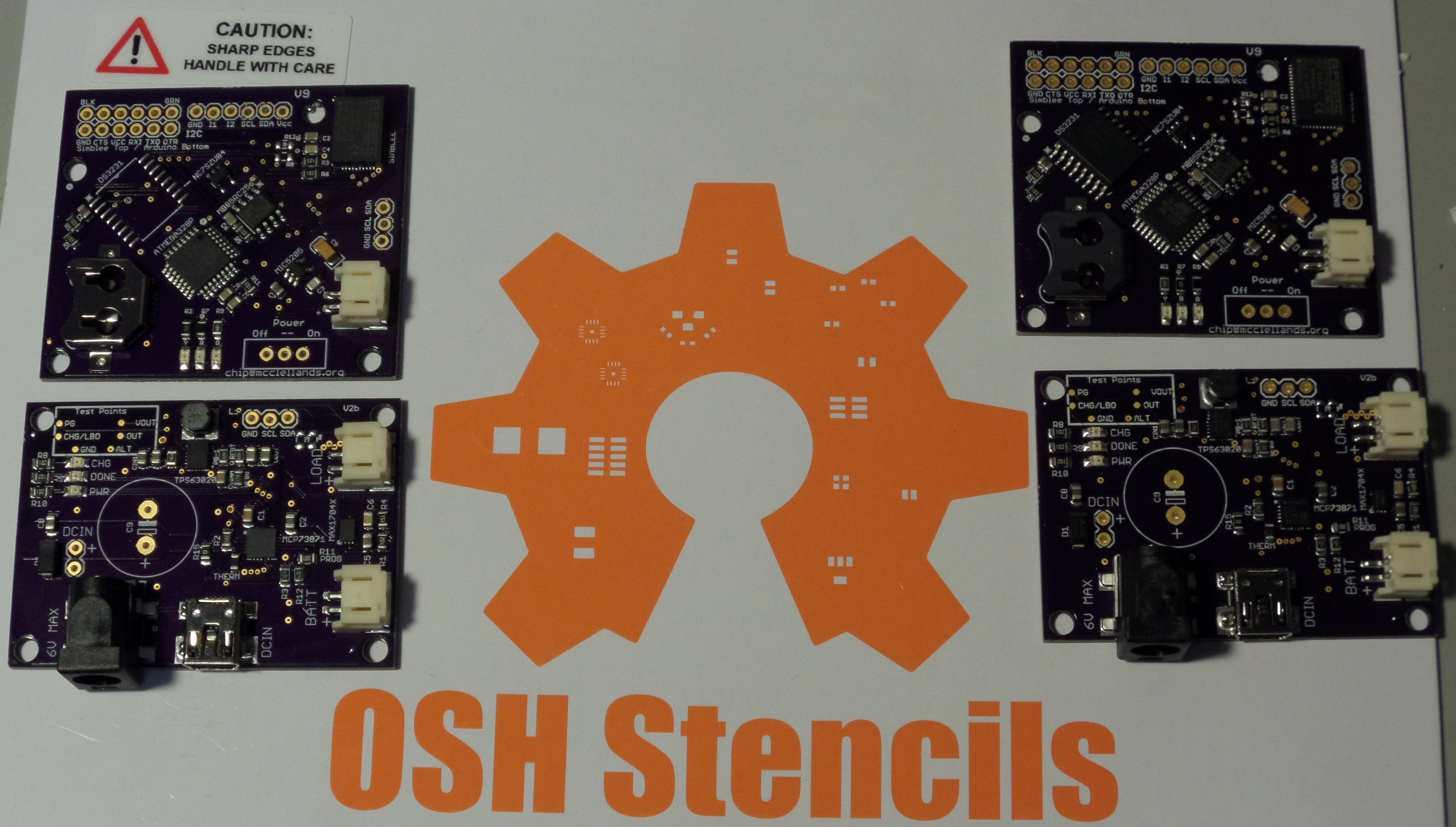
Here are Chip McClelland’s latest Trail Counter and Solar Charger boards, together with a shot of the stainless steel stencil now offered by OSH Stencils. The metal stencil makes it hugely easier to get perfect pasting and confirms that the curve that comes with polymide stencils has been at least one root cause of that type being so challenging to use. There was no paste bleed through to the back of the stencil, and the fine pitched power controller and Simblee BLE chip lands were perfectly formed. To get a sense of the cost difference some existing board specs were plugged into the OSH Stencils web site: a roughly five square inch battery charger, a three square inch decade counter/divider, and sub-square inch 6-axis breakout board. The steel stencils would be almost exactly double the cost of polymide, averaging about $12 each. By the way, multiple PCB designs can be grouped within one stencil. This can greatly reduce the cost difference depending on the areas involved.
These are OSH Park boards: very deep blue/purple, sitting on a sky blue antistatic mat. This is a tradeoff with the very bright, high color temperature LED flood lights used to illuminate the bench.
First Robotic Job Interview Caption Contest: WE HAVE A WINNER!
Atlas is looking for a job.
Winning caption for final scene of this video submitted by Carl Nobile:
“The Robot Counsel suggests that all people with hockey sticks should be jailed till we sort this out.”
See comments for other captions.
Need a Single Board Computer? Linux Gizmos has The List
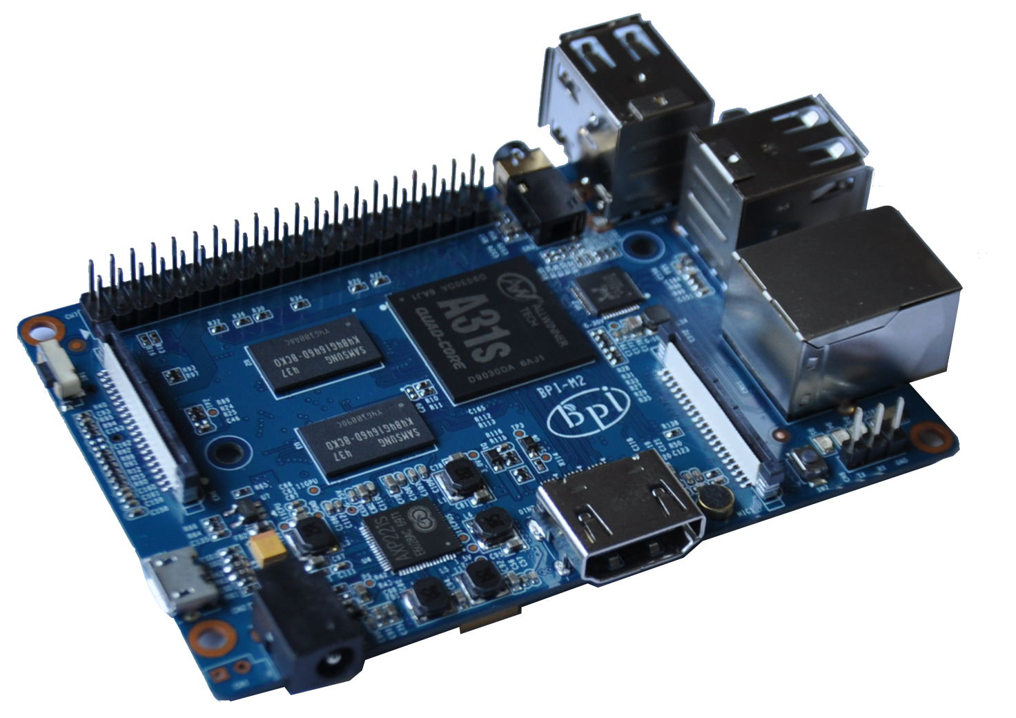
Linux Gizmos has assembled this list of 64 “open-spec, hacker friendly” single board computers.

