
2018 has a good chance of seeing embedded development accelerate sharply. Best wishes to the interest group and the wider community during this new year.

2018 has a good chance of seeing embedded development accelerate sharply. Best wishes to the interest group and the wider community during this new year.
GitHub, GitLab, and Atlassian BitBucket are all sites that offer git repository hosting. But if you create a repo named “Test” with BitBucket, then you copy/paste the slug URL and feed it to “git clone” as usual, the URL is forced to all lower case “test” and you end up with a clone of your repo in directory(folder) “test”. This stinks, for example, with common library directory naming conventions.
After thrashing around in the team settings, thinking I’d just missed the way to override the default URL, it occurred to me this might be a feature, not a bug. Sure enough:
https://jira.atlassian.com/browse/BSERV-3148
(“Stash” is simply Atlassian’s downloadable repo hosting system, effectively giving a customer a “Bitbucket” system within their enterprise)
This is just a classic bug report pattern. Who knows what caused the Bitbucket architect to decide not to honor the name spelling when creating the slug (the text box holding the URL you copy from to do a clone). But, the fact that one can simply modify the URL and end up with a target directory with any pattern of upper/lowercase makes it clear that they COULD offer an “honor name capitalization” radio button to override their sacred cow default, but they choose not to, with the lamest of lame excuses:
“Given that it is possible to modify the clone URL to include a camel-cased repository name (which creates a camel-cased repository directory when cloning), this is unlikely to be a priority in the near future.”
But this latest submission was started in 2013 and “resolved” in 2015, two years ago. Maybe it’s time to submit it again.
Archive of past meeting slides, videos, code and design files
A recent edition of “The Amp Hour” podcast had Chris and Dave interviewing “Sprite_tm” (aka Jeroen Domburg) of Espressif. Amongst all the other things this interesting Dutchman has accomplished, he added symmetric multiprocessing support to FreeRTOS on the ESP-32 (which has two identical 32 bit processors). I came completely unstitched hearing this toward the end of tantalizing news about the software tool chain available for this ESP8266 follow-on. Transparent multithreading with complete control over processor affinity (i.e. either bound or freely scheduled) was the final brush stroke painting a picture of superior infrastructure, open source accessibility and the usual unbeatable price point of the Espressif hardware. Wow.
Archive of past meeting slides, videos, code and design files
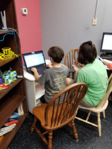
“I am Ben Goldberg, a 5th grader in Durham. I am proficient at programming in Arduino and Python and playing Pokemon GO. 😉
Come to the meeting and learn how to make a smart light that integrates with Apple HomeKit. This presentation, another Problem of the Month, and the usual discussions and show and tell are all in store. Meeting details
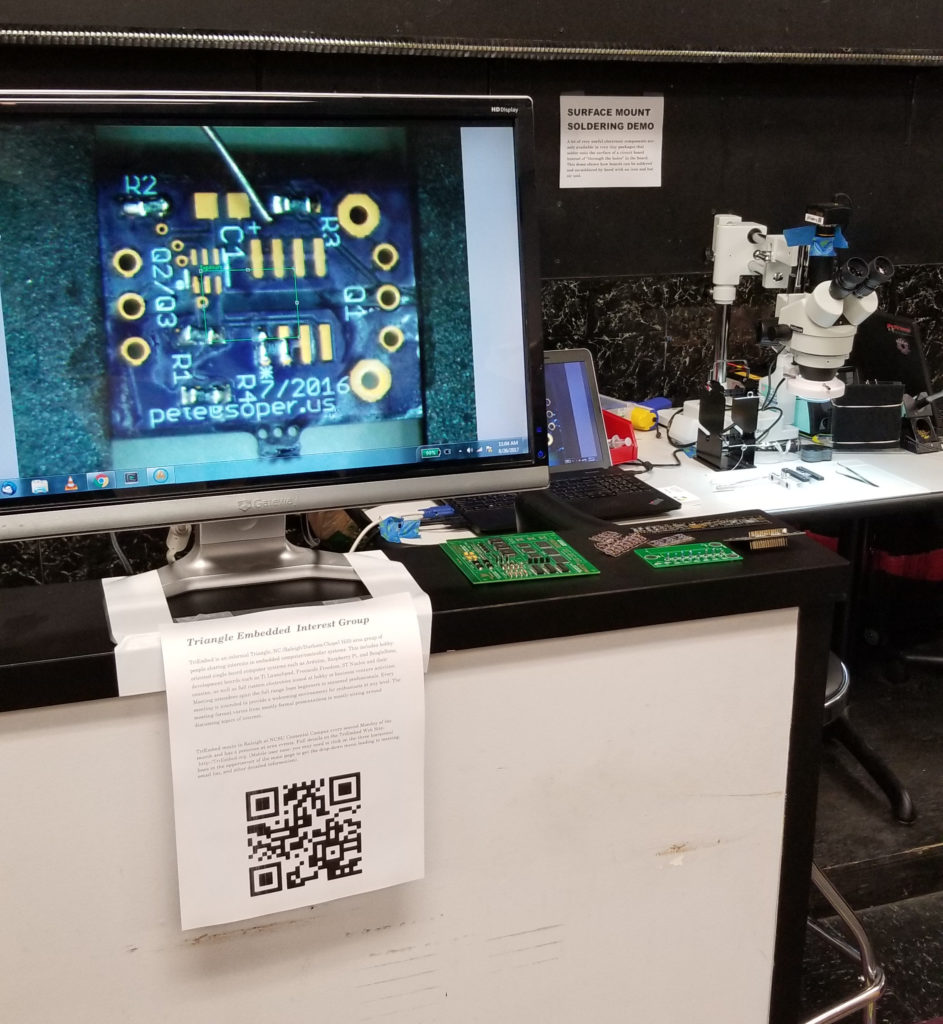
Today until 2pm is the second day of an open house of the area Triangle DIY Biology organization near Scrap Exchange in Durham. I was button-holed to “do something” at this event and decided the easiest thing to demonstrate would be how to hand solder fine pitch SMDs. TriEmbed info sheets are on hand and we’re also plugging SplatSpace. I’m using a little space at the popup to coordinate curation of Fred Ebeling’s Collection of electronic parts at SplatSpace.
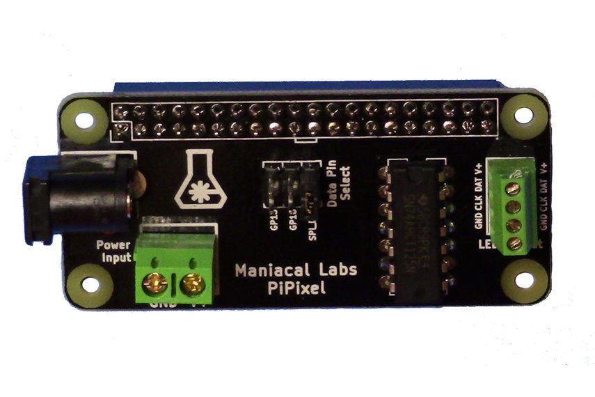
Adam Haile and Dan Ternes of Maniacal Labs have been busy. By accident I came across their site on Tindie and see they have a new product. PiPixel is oriented toward Raspberry Pi enthusiasts who would like to work with smart RGB LED strips. It’s described in detail on their web site. This is a super low cost kit that would make an excellent beginning soldering project with a big payoff. Find all the details on the ‘Labs web site.
As mentioned at the June 12th meeting, I find myself frequently wanting to find the sweet spot for quickly throwing a circuit together to see that gross behavior is as expected and confirm my assumptions correct and the devices perform as advertised before going to the trouble of making a PCB that is likely to be wrong if I’m in too much of a hurry.
But I sometimes find use of SMDs painful with solderless breadboards. First is the headache of having a parallel set of through-hole parts for bread boarding convenience. And of course this is an illusion in many cases: there are no through-hole equivalents for a growing number of components these days. Some shortfalls are obvious, like the current crop of tiny DC conversion chips that seem to be exploring the outer limits of how small a flat pack, no lead package can get. But others are chronic and might be surprising to some readers. Just try finding through-hole versions of some of the specific thermistor types specified for use with things like battery charger chips. It also gets old quick to have to buy a resistor with the same precision value in both through-hole and surface mount packages. And is that through-hole diode slapped on really behaving the same as the specific SMD spec’d for the “real implementation?”
I’ve been accumulating little breakout boards as carriers for various SMDs to make this easier, but that often involves a compromise, such as putting a tiny diode between two SOT-23 pads on a breakout that eats up six pins on a breadboard vs two. Other parts are more challenging and lead to semi-monstrosities like this one for a 22uH inductor:
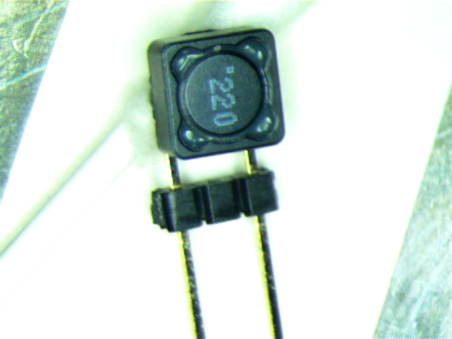
This is what a typical ad hoc collection of parts looks like:
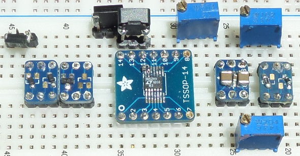
Notice the MSOP12 device is kludged onto a TSSOP14 breakout board. Also notice the (boost) capacitor soldered to the upper left pin of the MSOP12 package in the middle. It’s the barely noticeable bump on pin 12 of the IC (coincidentally below “12”, but electrically connected to header pin “14”, thus the error-prone kludge).
So, although my current breakout collection handles more than 30 devices directly, there are many gaps. This current project will bring the “package coverage” up around the 50 mark, but I estimate I’m only about half done before my hankering for this kind of support mostly dies down. For instance, there would be a lot to gain from handling the common form factors of small switches and connectors, small aluminum electrolytic caps, inductors, transistors, etc. Heck, there’s even real value in making an adaptor that saves me severely abusing a breadboard by cramming TO220 devices into the holes!
Adafruit and SparkFun and others provide some excellent breakout boards at affordable prices (in contrast to Schmartboard’s stuff, which seem to be both too much and too little for my needs). Notice all five of the boards above are Adafruit ones. I have several TI breakout types as well as others. But the actual coverage of package types for the available boards out there is too sparse.
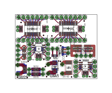
The aggregate PCB rendering above shows the approach I’m taking to build out my collection. This is a collection of 12 PCBs supporting 21 package types that I pulled together for the purpose of making stainless steel stencils. Some of the boards for larger parts have nearby pads for a few passives to make it less painful to handle bypass caps, boost caps, etc, where short connection paths are important.
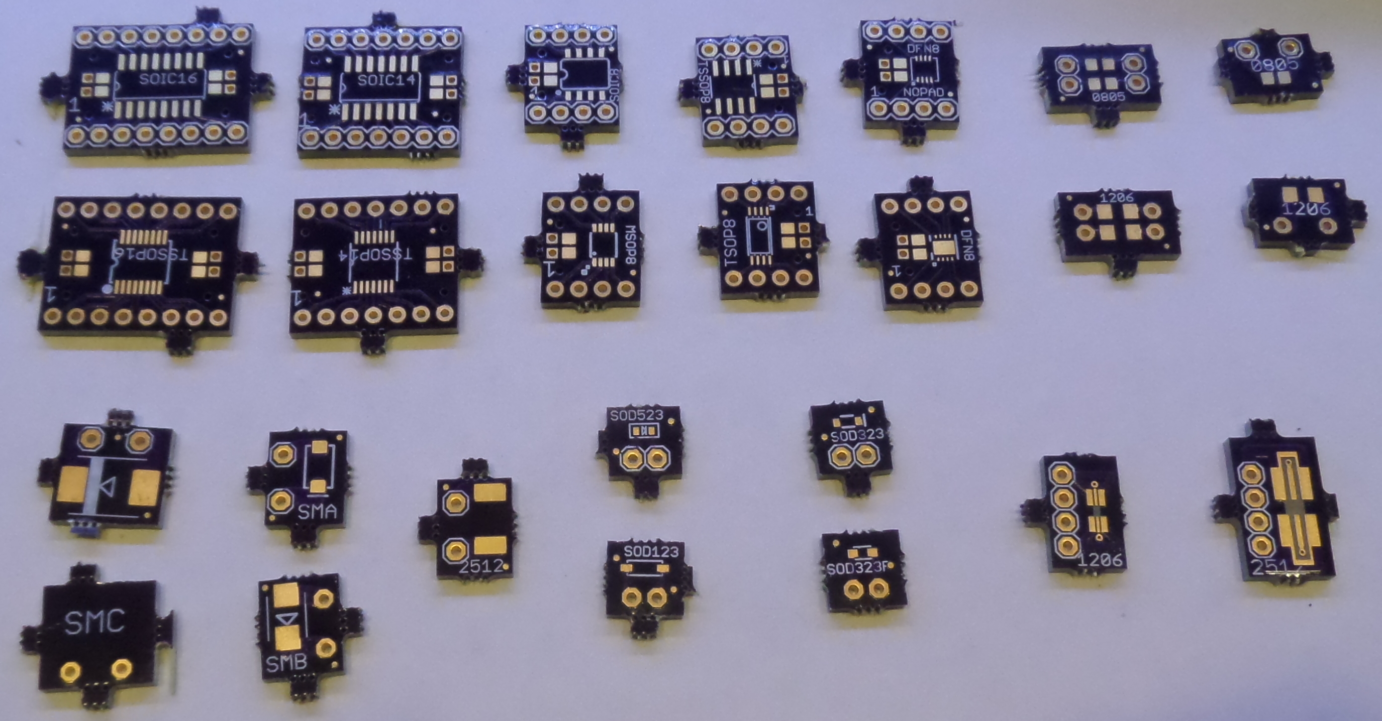
The 12 separate designs (and two others) were sent off to OSH Park to get three copies of each design as a small PCB so I can prove out the breakout boards .
Here is what the stencils from OSH Stencils look like for the top and bottom of the “aggregate PCB”:
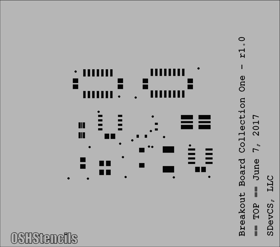
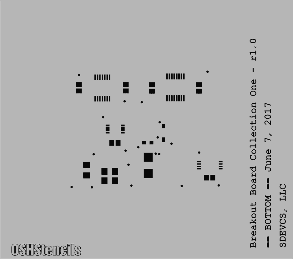
In theory, the work flow is to put the stencil over a particular breakout (e.g. the one for the SOIC14 package in the upper left corner of the top stencil). The one breakout PCB for the package is captured by a holder made of two acrylic “L” pieces vinyl-taped to a dead flat surface. A small squeegee (small piece of plastic credit card) is used to paste over the site(s) for a particular board, then parts are placed and hot air or reflow oven soldering is used.
A quick side note about frames. In many commercial environments the stencil is mounted in a surrounding frame that in turn fits into a jig allowing for rapid handling of boards while maintaining precise registration. I was confused Monday: OSH Stencils is only beta testing frame support with two sizes (relative to these boards those sizes are “wow”, and “my lawn is smaller than that”). Contact them for details if you’re interested.
I should also point out that I didn’t spend a lot of time routing these boards. For example, I’ve already had second thoughts about the sense line routes for the two shunt resistor boards that have ‘kelvin connections’ to special middle pads under the resistor ends. Also, as I mentioned Monday, I didn’t spend a lot of time checking things like length to width ratios for some stencil apertures. So the very narrow pad for the 1206 shunt board is technically smaller than the minimum supported size listed for the paste being used (Kester EP256), and the result may be that I can’t actually get paste into this spot properly. The footprint is blown up in the image below. The middle of each set of three pads is .28 millimeters wide. The resistor that sits on these pads is about an eighth of an inch long (yes, king size in relation to how these things are trending).
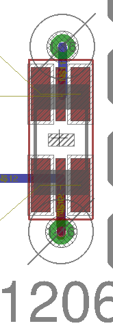
OK, but how much do those stencils cost? The minimum is $10, but the incremental cost beyond this is less than a dollar a square inch. The two stencils above came to around $22. First class postage with tracking adds $2.75 to an order. My order was completed on a Thursday and I had the stencils in hand the following Monday. With minimal (.75in) borders, everything you see in the first picture above added less than a dollar to each stencil cost. Note that in most cases you’ll only have a stencil for SMDs on one side.
(Update June 22nd)
The first batch of PCBs came back from OSH Park and are shown in the picture at the top of this posting. The tabs sticking out are cut off and squared off with sand paper before the boards are used.
Finally, it’s important to note that some circuits will not cooperate with solderless breadboards and any arrangement of surface mount parts involving long connection paths. Apart from huge amounts of stray inductive and capacitive reactance in the circuit paths, the current carrying limits of breadboards are very real, as is the ability of a simple breakout board to shed heat compared to a PCB having copper pours and other design features to properly handle it.